NCP3170
1
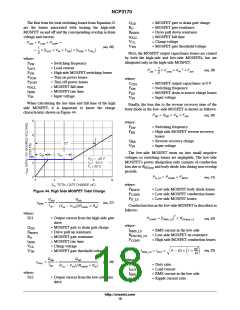
The first pole to crossover at the desired frequency should
be setup at FPO to decrease at −20 dB per decade:
RC
+
³
2p CC FP
(eq. 44)
FCROSS
1
2.925 kW +
FPO
+
³
2p 5.12 nF 1.512 kHz
G
(eq. 42)
50 kHz
33.061
where:
1.512 kHz +
³
C
C
F
= Compensation capacitance
= Output capacitance
= Current mode pole frequency
= Compensation resistor
C
OUT
P
where:
F
cross
F
PO
= Cross over frequency
= Pole frequency to meet crossover
frequency
R
C
1
CP
+
³
G
= DC gain of the plant
2p RC FESR
(eq. 45)
The crossover combined compensation network can be
used to calculate the transconductance output compensation
network as follows:
1
75.2 pF +
2p 2.925 kW 723 kHz
where:
y gm
C
P
= Compensation pole capacitor
= Capacitor ESR zero frequency
= Compensation resistor
CC
+
³
2 p FPO
F
ESR
(eq. 43)
R
C
0.242 200 ms
2p 1.512 kHz
5.12 nF +
If the ESR frequency is greater than the switching
frequency, a CF compensation capacitor may be needed for
stability as the output LC filter is considered high Q and thus
will not give the phase boost at the crossover frequency.
Further at low duty cycles due to some blanking and filtering
of the current signal the current gain of the converter is not
constant and the current gain is small. Thus adding CF and
RF can give the needed phase boost.
where:
C
C
= Compensation capacitor
= Pole frequency
= Transconductance of amplifier
= Amplitude ratio
F
PO
gm
y
R1 ) R2
CF
+
³
2p (R1 * RF ) R2 * RF ) R2 * R1) Fcross
(eq. 46)
24.9 kW ) 7.87 kW
456 pF +
2p (24.9 kW * 1 kW ) 7.87 kW * 1 kW ) 7.87 kW * 24.9 kW) 50 kHz
where:
IPK
C
F
= Compensation pole capacitor
= Cross over frequency
F
cross
gm
= Transconductance of amplifier
= Top resistor divider
= Bottom resistor divider
= Feed through resistor
R
1
R
2
R
F
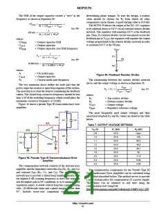
Figure 47. Input Charge Inrush Current
VIN
IICinrush_PK1 +
CINESR
Calculating Input Inrush Current
The input inrush current has two distinct stages: input
charging and output charging. The input charging of a buck
stage is usually controlled, but there are times when it is not
and is limited only by the input RC network, and the output
impedance of the upstream power stage. If the upstream
power stage is a perfect voltage source and switches on
instantaneously, then the input inrush current can be
depicted as shown in Figure 47 and calculated as:
(eq. 47)
12
1.2 kA +
0.01
VIN
5 CINESR CIN
IICinrush_RMS1 +
0.316
Ǹ
tDELAY_TOTAL
CINESR
(eq. 48)
12 V
5 0.01 W 22 mF
12.58 A +
0.316
Ǹ
0.01
1 ms
http://onsemi.com
22

 ONSEMI [ ONSEMI ]