NCP3170
The NCP3170 is the major source of power dissipation in
5. Create copper planes as short as possible from the
VSW pin to the output inductor, from the output
inductor to the output capacitor, and from the load
to PGND.
the system for which the equations above detailed the loss
mechanisms. The control portion of the IC power
dissipation is determined by the formula below:
6. Create a copper plane on all of the unused PCB
area and connect it to stable DC nodes such as:
PC + IC VIN
(eq. 52)
where:
V , GND, or V
.
IN
OUT
I
= Control circuitry current draw
= Control power dissipation
= Input voltage
CC
7. Keep sensitive signal traces far away from the
VSW pins or shield them.
P
C
V
IN
Once the IC power dissipations are determined, the
designer can calculate the required thermal impedance to
maintain a specified junction temperature at the worst case
ambient temperature. The formula for calculating the
junction temperature with the package in free air is:
TJ + TA ) PD RqJA
(eq. 53)
where:
P
D
= Power dissipation of the IC
R
qJA
= Thermal resistance junction to ambient
of the regulator package
T
A
= Ambient temperature
T
= Junction temperature
J
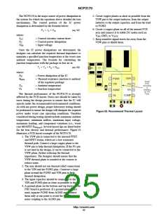
The thermal performance of the NCP3170 is strongly
affected by the PCB layout. Extra care should be taken by
users during the design process to ensure that the IC will
operate under the recommended environmental conditions.
As with any power design, proper laboratory testing should
be performed to ensure the design will dissipate the required
power under worst case operating conditions. Variables
considered during testing should include maximum ambient
temperature, minimum airflow, maximum input voltage,
maximum loading, and component variations (i.e., worst
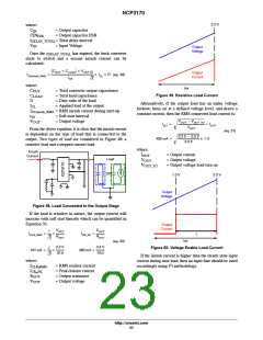
Figure 53. Recommend Thermal Layout
case MOSFET R ). Several layout tips are listed below
DS(on)
for the best electric and thermal performance. Figure 53
illustrates a PCB layout example of the NCP3170.
1. The VSW pin is connected to the internal PFET
and NFET drains, which are a low resistance
thermal path. Connect a large copper plane to the
VSW pin to help thermal dissipation. If the PG pin
is not used in the design, it can be connected to the
VSW plane, further reducing the thermal
impedance. The designer should ensure that the
VSW thermal plane is rounded at the corners to
reduce noise.
2. The user should not use thermal relief connections
to the VIN and the PGND pins. Construct a large
plane around the PGND and VIN pins to help
thermal dissipation.
3. The input capacitor should be connected to the
VIN and PGND pins as close as possible to the IC.
4. A ground plane on the bottom and top layers of the
PBC board is preferred. If a ground plane is not
used, separate PGND from AGND and connect
them only at one point to avoid the PGND pin
noise coupling to the AGND pin.
http://onsemi.com
25

 ONSEMI [ ONSEMI ]