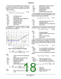
NCP3170
The first term for total switching losses from Equation 25
are the losses associated with turning the high-side
MOSFET on and off and the corresponding overlap in drain
voltage and current.
Q
= MOSFET gate to drain gate charge
= MOSFET gate resistance
= Drive pull down resistance
= MOSFET fall time
GD
G
R
R
HSPD
FALL
t
V
V
= Clamp voltage
= MOSFET gate threshold voltage
CL
TH
PSW + PTON ) PTOFF
+
(eq. 26)
1
ǒ
Ǔ
ǒ
Ǔ
+
IOUT VIN FSW tRISE ) tFALL
2
Next, the MOSFET output capacitance losses are caused
by both the high-side and low-side MOSFETs, but are
dissipated only in the high-side MOSFET.
where:
F
I
= Switching frequency
= Load current
SW
1
OUT
2
(eq. 29)
PDS
+
COSS VIN FSW
P
= High side MOSFET switching losses
= Turn on power losses
= Turn off power losses
= MOSFET fall time
2
SW
P
P
TON
TOFF
FALL
RISE
where:
C
= MOSFET output capacitance at 0 V
= Switching frequency
= MOSFET drain to source charge losses
= Input voltage
OSS
SW
DS
t
t
F
P
= MOSFET rise time
V
IN
= Input voltage
V
IN
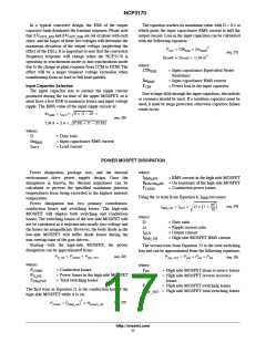
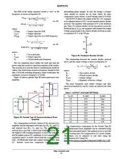
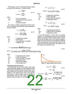
When calculating the rise time and fall time of the high
side MOSFET, it is important to know the charge
characteristic shown in Figure 44.
Finally, the loss due to the reverse recovery time of the
body diode in the low−side MOSFET is shown as follows:
PRR + QRR VIN FSW
(eq. 30)
where:
F
SW
P
RR
= Switching frequency
= High side MOSFET reverse recovery
losses
Q
RR
V
IN
= Reverse recovery charge
= Input voltage
The low-side MOSFET turns on into small negative
voltages so switching losses are negligible. The low-side
MOSFET’s power dissipation only consists of conduction
Vth
loss due to R
periods.
and body diode loss during non-overlap
DS(on)
PD_LS + PCOND ) PBODY
(eq. 31)
where:
P
P
P
= Low side MOSFET body diode losses
= Low side MOSFET conduction losses
= Low side MOSFET losses
BODY
COND
D_LS
Figure 44. High Side MOSFET Total Charge
QGD
IG1
QGD
tRISE
+
+
(eq. 27)
ǒ
Ǔ ǒ
Ǔ
Conduction loss in the low-side MOSFET is described as
VCL * VTH ń RHSPU ) RG
follows:
where:
IG1
ǒ
Ǔ2
= Output current from the high-side gate
drive
= MOSFET gate to drain gate charge
= Drive pull up resistance
= MOSFET gate resistance
= MOSFET rise time
PCOND + IRMS_LS RDS(on)_LS
(eq. 32)
where:
Q
GD
I
= RMS current in the low side
= Low-side MOSFET on resistance
= High side MOSFET conduction losses
RMS_LS
R
HSPU
R
G
R
P
DS(ON)_LS
COND
t
RISE
V
V
= Clamp voltage
= MOSFET gate threshold voltage
CL
TH
ra2
Ǹ
ǒ1 )
Ǔ
(eq. 33)
( )
1 * D
IRMS_LS + IOUT
12
QGD
QGD
where:
D
tFALL
+
+
(eq. 28)
IG2
= Duty ratio
= Load current
ǒ
Ǔ ǒ
Ǔ
VCL * VTH ń RHSPD ) RG
I
I
OUT
where:
IG2
= RMS current in the low side
= Ripple current ratio
RMS_LS
= Output current from the low-side gate
drive
ra
http://onsemi.com
18

 ONSEMI [ ONSEMI ]