NCP3170
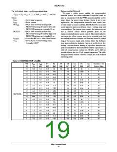
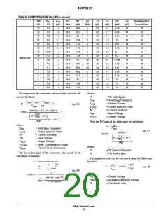
Table 6. COMPENSATION VALUES (continued)
VIN
(V)
V
L
R1
R2
Rf
Cf
Cc
Rc
Cp
Resistance for
Current Gain
out
out
(V)
1.2
1.5
1.8
2.5
3.3
5.0
10.68
14.8
0.8
1.0
1.1
1.2
1.5
1.8
2.5
3.3
(mF)
1.5
1.8
1.8
2.7
3.3
3.3
1.5
3.3
1.0
1.0
1.0
1.5
1.5
1.5
1.8
1.8
(kW)
(kW)
49.9
28.7
20
(kW)
(pF)
(nF)
(kW)
(pF)
12
12
12
12
12
12
12
18
5
24.9
24.9
24.9
24.9
24.9
24.9
24.9
24.9
24.9
24.9
24.9
24.9
24.9
24.9
24.9
24.9
1
1
82
82
82
82
82
82
82
82
NI
NI
NI
82
82
82
82
82
2.7
2.7
2.7
1.8
1.5
2.2
2.2
2.2
15
6.04
6.04
6.04
10
NI
NI
NI
NI
NI
NI
NI
NI
NI
NI
NI
NI
NI
NI
NI
NI
20
22
22
32
52
52
52
52
20
28
42
55
55
55
55
55
1
11.8
7.87
4.75
2.05
1.43
NI
1
1
12.1
8.25
5.1
1
1
1
5.1
NCP3170B
NI
NI
NI
1
0.499
1.69
3.61
6.04
6.04
10
5
100
66.5
49.9
28.7
20
6.8
3.9
2.7
2.7
1.8
1.8
1.8
5
5
5
1
5
1
5
11.8
7.87
1
10
5
1
10
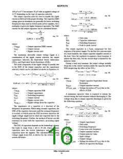
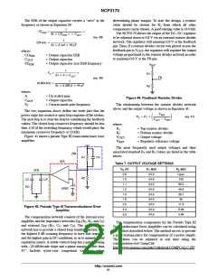
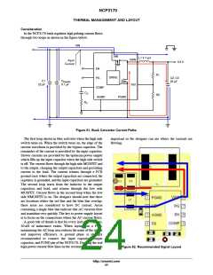
To compensate the converter we must first calculate the
current feedback
where:
A
= Un-scaled gain
F
I
L
M
V
V
= Switching Frequency
= Output Current
= Output inductor value
= Current feedback
= Input Voltage
SW
F
L
V
OUT
RAMP
SW
M +
) 1 ³
(eq. 35)
OUT
R
VIN
MAP
OUT
500 kHz 4.7 mH 0.33 V
7.299 +
) 1
IN
3.3 V
32
12 V)1.46
1000
ǒ
Ǔ
W 12 V
= Output Voltage
OUT
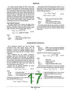
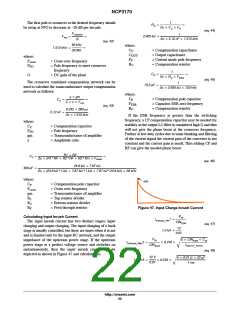
Next the DC gain of the plant must be calculated.
where:
A
G +
³
RMAP
F
SW
= Switching Frequency
= Output inductor value
= Current feedback
= Input Voltage
= Output Voltage
(eq. 37)
L
OUT
0.339 W
33.016 +
M
Vin
3.3 V
32
12 V)1.46
ǒ
Ǔ
W
V
V
R
OUT
1000
= Slope Compensation Ramp
= Current Sense Resistance
RAMP
MAP
where:
G
A
= DC gain of the plant
= Un−scaled gain
The un-scaled gain of the converter also needs to be
calculated as follows:
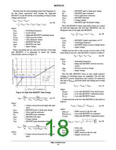
The amplitude ratio can be calculated using the following
equation:
1
A +
VOUT
M*0.5*M
0.8 V
VREF
VOUT
IOUT
VIN
Y +
³ 0.242 +
(eq. 38)
)
)
VOUT
LOUT FSW
3.3 V
(eq. 36)
1
where:
Vo
VREF
0.339 W +
3.3 V
12 V
= Output voltage
= Regulator reference voltage
= Amplitude ratio
7.299*0.5*7.299
3.0 A
3.3 V
4.7 mH 500 kHz
Y
http://onsemi.com
20

 ONSEMI [ ONSEMI ]