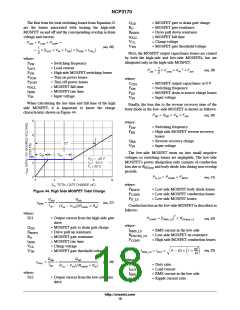
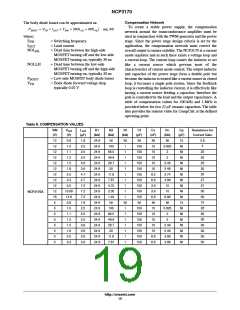
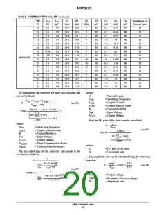
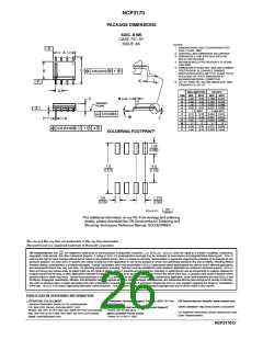
NCP3170
THERMAL MANAGEMENT AND LAYOUT
Consideration
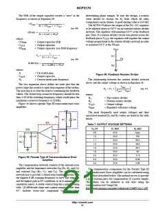
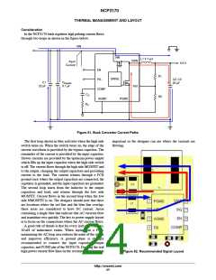
In the NCP3170 buck regulator high pulsing current flows
through two loops as shown in the figure below.
VIN
VIN
L1 4.7 mH
VSW
FB1
Input
Current
3.3 V
EN
PG
R1
R2
DRIVE
C2, C3
22 mF
C1
22 mF
C
bypass
0.1 mF
COMP
AGND
C
C
PGND
R
C
Figure 51. Buck Converter Current Paths
The first loop shown in blue activates when the high side
switch turns on. When the switch turns on, the edge of the
current waveform is provided by the bypass capacitor. The
remainder of the current is provided by the input capacitor.
Slower currents are provided by the upstream power supply
which fills up the input capacitor when the high side switch
is off. The current flows through the high side MOSFET and
to the output, charging the output capacitors and providing
current to the load. The current returns through a PCB
ground trace where the output capacitors are connected, the
regulator is grounded, and the input capacitors are grounded.
The second loop starts from the inductor to the output
capacitors and load, and returns through the low side
MOSFET. Current flows in the second loop when the low
side NMOSFET is on. The designer should note that there
are locations where the red line and the blue line overlap;
these areas are considered to have DC current. Areas
containing a single blue line indicate that AC currents flow
and transition very quickly. The key to power supply layout
is to focus on the connections where the AC current flows.
A good rule of thumb is that for every inch of PCB trace,
20 nH of inductance exists. When laying out a PCB,
minimizing the AC loop area reduces the noise of the circuit
and improves efficiency. A ground plane is strongly
recommended to connect the input capacitor, output
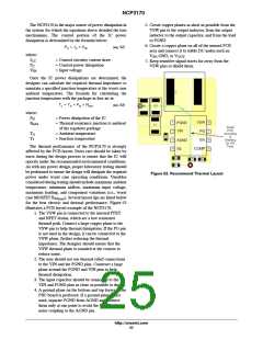
capacitor, and PGND pin of the NCP3170. Drawing the real
high power current flow lines on the recommended layout is
important so the designer can see where the currents are
flowing.
Figure 52. Recommended Signal Layout
http://onsemi.com
24

 ONSEMI [ ONSEMI ]