NCP3170
In a typical converter design, the ESR of the output
capacitor bank dominates the transient response. Please note
that DV and DV are out of phase with each
The equation reaches its maximum value with D = 0.5 at
which point the input capacitance RMS current is half the
output current. Loss in the input capacitors can be calculated
with the following equation:
_
OUT DIS
OUT_ESR
other, and the larger of these two voltages will determine the
maximum deviation of the output voltage (neglecting the
effect of the ESL). It is important to note that the converters
frequency response will change when the NCP3170 is
operating in synchronous mode or non-synchronous mode
due to the change in plant response from CCM to DCM. The
effect will be a larger transient voltage excursion when
transitioning from no load to full load quickly.
ǒ
Ǔ2
PCIN + CINESR IinRMS
(eq. 21)
ǒ
Ǔ2
18 mW + 10 mW 1.34 A
where:
CIN
= Input capacitance Equivalent Series
Resistance
ESR
Iin
= Input capacitance RMS current
= Power loss in the input capacitor
RMS
Input Capacitor Selection
P
CIN
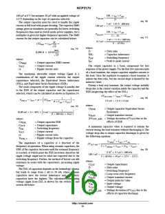
The input capacitor has to sustain the ripple current
produced during the on time of the upper MOSFET, so it
must have a low ESR to minimize losses and input voltage
ripple. The RMS value of the input ripple current is:
Due to large di/dt through the input capacitors, electrolytic
or ceramics should be used. If a tantalum capacitor must be
used, it must be surge protected, otherwise capacitor failure
could occur.
Ǹ
( )
D 1 * D ³
IinRMS + IOUT
(eq. 20)
Ǹ
(
)
1.34 A + 3 A 27.5% 1 * 27.5%
where:
D
= Duty ratio
Iin
= Input capacitance RMS current
= Load current
RMS
I
OUT
POWER MOSFET DISSIPATION
where:
Power dissipation, package size, and the thermal
environment drive power supply design. Once the
dissipation is known, the thermal impedance can be
calculated to prevent the specified maximum junction
temperatures from being exceeded at the highest ambient
temperature.
Power dissipation has two primary contributors:
conduction losses and switching losses. The high-side
MOSFET will display both switching and conduction
losses. The switching losses of the low side MOSFET will
not be calculated as it switches into nearly zero voltage and
the losses are insignificant. However, the body diode in the
low-side MOSFET will suffer diode losses during the
non-overlap time of the gate drivers.
I
R
P
= RMS current in the high side MOSFET
= On resistance of the high side MOSFET
= Conduction power losses
RMS_HS
DS(ON)_HS
COND
Using the ra term from Equation 6, I
becomes:
RMS
ra2
ǸD ǒ1 )
Ǔ
(eq. 24)
IRMS_HS + IOUT
12
where:
D
ra
I
I
= Duty ratio
= Ripple current ratio
= Output current
OUT
= High side MOSFET RMS current
RMS_HS
Starting with the high-side MOSFET, the power
dissipation can be approximated from:
The second term from Equation 22 is the total switching
loss and can be approximated from the following equations.
PD_HS + PCOND ) PSW_TOT
(eq. 22)
PSW_TOT + PSW ) PDS ) PRR
(eq. 25)
where:
P
where:
= Conduction losses
= Power losses in the high side MOSFET
= Total switching losses
P
DS
= High side MOSFET drain to source losses
= High side MOSFET reverse recovery
losses
COND
P
P
P
RR
D_HS
SW_TOT
P
P
= High side MOSFET switching losses
= High side MOSFET total switching losses
SW
The first term in Equation 21 is the conduction loss of the
high-side MOSFET while it is on.
SW_TOT
Ǔ2
(eq. 23)
ǒ
PCOND + IRMS_HS RDS(on)_HS
http://onsemi.com
17

 ONSEMI [ ONSEMI ]