NCP3170
ESL IPP FSW
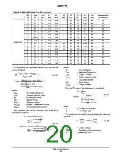
100 mF at 0 V but measure 20 mF with an applied voltage of
VESLON
+
³
3.3 V depending on the type of capacitor selected.
The output capacitor must be rated to handle the ripple
current at full load with proper derating. The capacitor RMS
ratings given in datasheets are generally for lower switching
frequencies than used in switch mode power supplies, but a
multiplier is given for higher frequency operation. The RMS
current for the output capacitor can be calculated below:
ra
D
(eq. 16)
(eq. 17)
1 nH @ 1.01 A @ 500 kHz
1.84 mV +
27.5%
ESL IPP FSW
VESLOFF
+
³
(
)
1 * D
1 nH 1.1 A 500 kHz
0.7 mV +
(
)
1 * 27.5%
CORMS + I
³
OUT Ǹ
12
where:
D
ESL
(eq. 14)
34%
= Duty ratio
0.294 A + 3.0 A
Ǹ
= Capacitor inductance
= Switching frequency
= Peak-to-peak current
12
F
SW
PP
where:
Co
I
= Output capacitor RMS current
= Output current
RMS
I
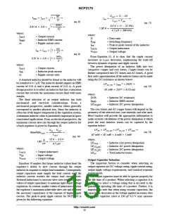
The output capacitor is a basic component for fast
response of the power supply. For the first few microseconds
of a load transient, the output capacitor supplies current to
the load. Once the regulator recognizes a load transient, it
adjusts the duty ratio, but the current slope is limited by the
inductor value.
During a load step transient, the output voltage initially
drops due to the current variation inside the capacitor and the
ESR (neglecting the effect of the ESL).
OUT
ra
= Ripple current ratio
The maximum allowable output voltage ripple is a
combination of the ripple current selected, the output
capacitance selected, the Equivalent Series Inductance
(ESL), and Equivalent Series Resistance (ESR).
The main component of the ripple voltage is usually due
to the ESR of the output capacitor and the capacitance
selected, which can be calculated as shown in Equation 14:
DVOUT−ESR + ITRAN COESR
³
(eq. 18)
1
ǒ
Ǔ
VESR_C + IOUT ra COESR
)
³
7.5 mV + 1.5 A 5 mW
8 FSW COUT
where:
(eq. 15)
Co
= Output capacitor Equivalent Series
Resistance
= Output transient current
= Voltage deviation of V
effects of ESR
ESR
1
ǒ5 mW )
Ǔ
10.89 mV + 3 34%
8 500 kHz 44 mF
I
TRAN
ąDV
_
due to the
where:
OUT ESR
OUT
Co
C
F
= Output capacitor ESR
= Output capacitance
= Switching frequency
= Output current
ESR
OUT
SW
A minimum capacitor value is required to sustain the
current during the load transient without discharging it. The
voltage drop due to output capacitor discharge is given by
the following equation:
I
OUT
ra
= Ripple current ratio
= Ripple voltage from the capacitor
V
ESR_C
ǒ
Ǔ2
ITRAN LOUT FSW
The impedance of a capacitor is a function of the
frequency of operation. When using ceramic capacitors, the
ESR of the capacitor decreases until the resonant frequency
is reached, at which point the ESR increases; therefore the
ripple voltage might not be what one expected due to the
switching frequency. Further, the method of layout can add
resistance in series with the capacitance, increasing ripple
voltage.
The ESL of capacitors depends on the technology chosen,
but tends to range from 1 nH to 20 nH, where ceramic
capacitors have the lowest inductance and electrolytic
capacitors have the highest. The calculated contributing
voltage ripple from ESL is shown for the switch on and
switch off below:
DVOUT−DIS
+
³
ǒ
Ǔ
2 FCROSS COUT VIN * VOUT
(eq. 19)
2
(
)
1.5 4.7 mH 500 kHz
138.1 mV +
ǒ
Ǔ
2 50 kHz 44 mF 12 V * 3.3 V
where:
C
OUT
= Output capacitance
= Duty ratio
D
F
F
= Switching frequency
= Loop cross over frequency
= Output transient current
= Output inductor value
= Input voltage
SW
CROSS
TRAN
I
L
OUT
V
V
IN
= Output voltage
OUT
ąDV
_
= Voltage deviation of V
due to the
OUT DIS
OUT
effects of capacitor discharge
http://onsemi.com
16

 ONSEMI [ ONSEMI ]