NCP3170
ra2
12
(
)
VOUT 1 * D
Ǹ1 )
Ǹ1 )
IRMS + IOUT
³
IPP
+
³
LOUT FSW
(eq. 8)
(eq. 11)
34%2
12
(
)
3.3 V 1 * 27.5%
3.01 A + 3 A
³
1.02 A +
4.7 mH 500 kHz
where:
where:
D
I
I
= Output current
= Inductor RMS current
= Ripple current ratio
OUT
= Duty ratio
= Switching frequency
RMS
F
SW
PP
ra
I
= Peak-to-peak current of the inductor
= Output inductance
= Output voltage
L
V
ǒ1 ) raǓ
OUT
IPK + IOUT
³
OUT
2
(eq. 9)
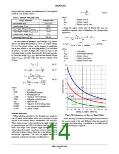
From Equation 11, it is clear that the ripple current
increases as L decreases, emphasizing the trade-off
between dynamic response and ripple current.
3.51 A + 3 A ǒ1 ) 34%Ǔ
OUT
2
where:
The power dissipation of an inductor falls into two
categories: copper and core losses. Copper losses can be
further categorized into DC losses and AC losses. A good
first order approximation of the inductor losses can be made
using the DC resistance as shown below:
I
I
= Output current
= Inductor peak current
= Ripple current ratio
OUT
PK
ra
A standard inductor should be found so the inductor will
be rounded to 4.7 mH. The inductor should support an RMS
current of 3.01 A and a peak current of 3.51 A. A good
design practice is to select an inductor that has a saturation
current that exceeds the maximum current limit with some
margin.
2
LPCU_DC + IRMS DCR ³
(eq. 12)
61 mW + 3.012 6.73 mW
where:
DCR
= Inductor DC resistance
= Inductor RMS current
The final selection of an output inductor has both
mechanical and electrical considerations. From
I
RMS
a
LP
= Inductor DC power dissipation
CU_DC
mechanical perspective, smaller inductor values generally
correspond to smaller physical size. Since the inductor is
often one of the largest components in the regulation system,
a minimum inductor value is particularly important in space
constrained applications. From an electrical perspective, the
maximum current slew rate through the output inductor for
a buck regulator is given by Equation 10.
The core losses and AC copper losses will depend on the
geometry of the selected core, core material, and wire used.
Most vendors will provide the appropriate information to
make accurate calculations of the power dissipation at which
point the total inductor losses can be captured by the
equation below:
LPtot + LPCU_DC ) LPCU_AC ) LPCore
³
VIN * VOUT
(eq. 13)
SlewRateLOUT
+
+
³
LOUT
67 mW + 61 mW ) 5 mW ) 1 mW
(eq. 10)
12 V * 3.3 V
4.7 mH
where:
LP
A
1.85
ms
= Inductor core power dissipation
= Inductor AC power dissipation
= Inductor DC power dissipation
= Total inductor losses
Core
LP
LP
LP
CU_AC
CU_DC
tot
where:
L
= Output inductance
= Input voltage
OUT
V
V
IN
= Output voltage
OUT
Output Capacitor Selection
The important factors to consider when selecting an
output capacitor are DC voltage rating, ripple current rating,
output ripple voltage requirements, and transient response
requirements.
The output capacitor must be able to operate properly for
the life time of a product. When selecting a capacitor it is
important to select a voltage rating that is de-rated to the
guaranteed operating life time of a product. Further, it is
important to note that when using ceramic capacitors, the
capacitance decreases as the voltage applied increases; thus
a ceramic capacitor rated at 100 mF 6.3 V may measure
Equation 10 implies that larger inductor values limit the
regulator’s ability to slew current through the output
inductor in response to output load transients. Consequently,
output capacitors must supply the load current until the
inductor current reaches the output load current level.
Reduced inductance to increase slew rates results in larger
values of output capacitance to maintain tight output voltage
regulation. In contrast, smaller values of inductance increase
the regulator’s maximum achievable slew rate and decrease
the necessary capacitance at the expense of higher ripple
current. The peak-to-peak ripple current for NCP3170 is
given by the following equation:
http://onsemi.com
15

 ONSEMI [ ONSEMI ]