NCP3170
design point and optimize the performance of your regulator
based on your design criteria.
DI
ra +
(eq. 6)
IOUT
where:
ąDI
Table 5. DESIGN PARAMETERS
Design Parameter
= Ripple current
= Output current
= Ripple current ratio
Example Value
9 V to 16 V
3.3 V
I
OUT
Input Voltage (V
)
IN
ra
Output Voltage (V
)
OUT
Using the ripple current rule of thumb, the user can
establish acceptable values of inductance for a design using
Equation 6.
Input Ripple Voltage (VCC
)
200 mV
20 mV
RIPPLE
Output Ripple Voltage (V
)
OUTRIPPLE
Output Current Rating (I
Operating Frequency (F
)
3 A
OUT
VOUT
( )
1 * D ³
)
500 kHz
LOUT
+
SW
IOUT ra FSW
(eq. 7)
The buck converter produces input voltage (V ) pulses
that are LC filtered to produce a lower DC output voltage
IN
12 V
( )
1 * 27.5%
4.7 mH +
3.0 A 34% 500 kHz
(V ). The output voltage can be changed by modifying
OUT
the on time relative to the switching period (T) or switching
frequency. The ratio of high side switch on time to the
switching period is called duty ratio (D). Duty ratio can also
where:
D
= Duty ratio
= Switching frequency
= Output current
= Output inductance
= Ripple current ratio
F
SW
be calculated using V , V , the Low Side Switch Voltage
OUT IN
I
OUT
Drop (V
), and the High Side Switch Voltage Drop
LSD
L
OUT
(V
).
HSD
ra
1
(eq. 3)
(eq. 4)
FSW
TON
+
19
T
TOFF
T
17
15
13
11
9
(
)
1 * D +
D +
D +
T
VOUT ) VLSD
VIN * VHSD ) VLSD
[
(eq. 5)
VOUT
VIN
3.3 V
12 V
D +
³ 27.5% +
18 V
where:
D
FSW
T
TOFF
TON
= Duty ratio
7 V
= Switching frequency
= Switching period
= High side switch off time
= High side switch on time
= Input voltage
= High side switch voltage drop
= Low side switch voltage drop
= Output voltage
7
4.7 mH
5
V
IN
3
VHSD
VLSD
VOUT
4.4 V
1
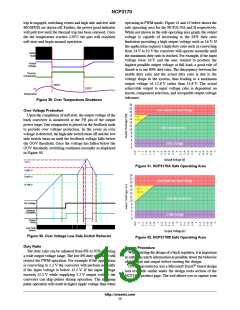
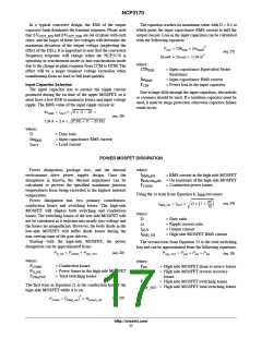
10 13 16 19 22 25 28 31 34 37 40
RIPPLE CURRENT RATIO (%)
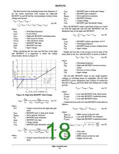
Inductor Selection
Figure 43. Inductance vs. Current Ripple Ratio
When selecting an inductor, the designer may employ a
rule of thumb for the design where the percentage of ripple
current in the inductor should be between 10% and 40%.
When using ceramic output capacitors, the ripple current can
be greater because the ESR of the output capacitor is smaller,
thus a user might select a higher ripple current. However,
when using electrolytic capacitors, a lower ripple current
will result in lower output ripple due to the higher ESR of
electrolytic capacitors. The ratio of ripple current to
maximum output current is given in Equation 6.
When selecting an inductor, the designer must not exceed
the current rating of the part. To keep within the bounds of
the part’s maximum rating, a calculation of the RMS current
and peak current are required.
http://onsemi.com
14

 ONSEMI [ ONSEMI ]