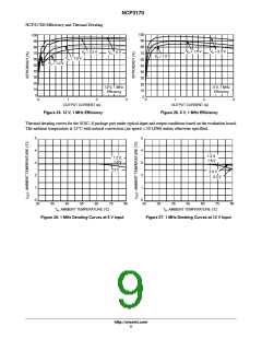
NCP3170
trip is engaged, switching ceases and high side and low side
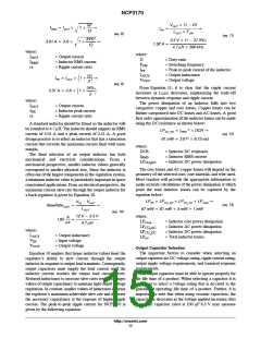
operating in PWM mode. Figure 41 and 42 below shows the
safe operating area for the NCP3170A and B respectively.
While not shown in the safe operating area graph, the output
voltage is capable of increasing to the 93% duty ratio
limitation providing a high output voltage such as 16 V. If
the application requires a high duty ratio such as converting
from 14 V to 10 V the converter will operate normally until
the maximum duty ratio is reached. For example, if the input
voltage were 16 V and the user wanted to produce the
highest possible output voltage at full load, a good rule of
thumb is to use 80% duty ratio. The discrepancy between the
usable duty ratio and the actual duty ratio is due to the
voltage drops in the system, thus leading to a maximum
output voltage of 12.8 V rather than 14.8 V. The actual
achievable output to input voltage ratio is dependent on
layout, component selection, and acceptable output voltage
tolerance.
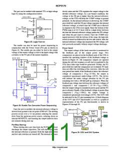
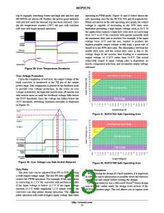
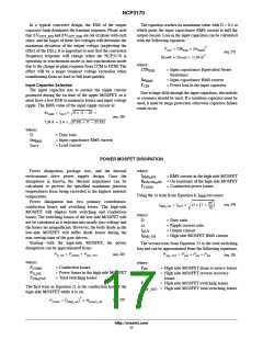
MOSFETs are driven off. Further, the power good indicator
will pull low until the thermal trip has been released. Once
the die temperature reaches 120°C the part will reinitiate
soft-start and begin normal operation.
Switch
Node
Output
Voltage
Thermal
Comparator
150°C
120°C
IC
Temperature
Figure 39. Over Temperature Shutdown
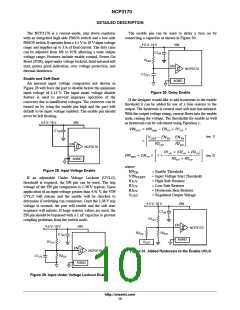
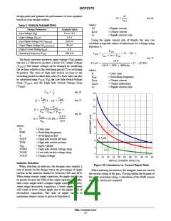
Over Voltage Protection
Upon the completion of soft start, the output voltage of the
buck converter is monitored at the FB pin of the output
power stage. One comparator is placed on the feedback node
to provide over voltage protection. In the event an over
voltage is detected, the high side switch turns off and the low
side switch turns on until the feedback voltage falls below
the OOV threshold. Once the voltage has fallen below the
OOV threshold, switching continues normally as displayed
in Figure 40.
1.0 V
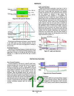
Figure 41. NCP3170A Safe Operating Area
0.862 V
0.800 V
0.726 V
FB Voltage
Softstart
Complete
Power
Good
Low Side
Switch
Figure 40. Over Voltage Low Side Switch Behavior
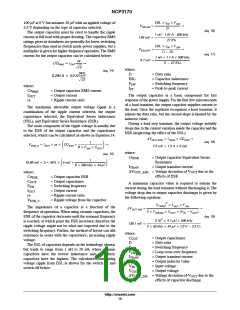
Figure 42. NCP3170B Safe Operating Area
Duty Ratio
Design Procedure
The duty ratio can be adjusted from 8% to 92% allowing
a wide output voltage range. The low 8% duty ratio limit will
restrict the PWM operation. For example if the application
is converting to 1.2 V the converter will perform normally
if the input voltage is below 15.5 V. If the input voltage
exceeds 15.5 V while supplying 1.2 V output voltage the
converter can skip pulses during operation. The skipping
pulse operation will result in higher ripple voltage than when
When starting the design of a buck regulator, it is important
to collect as much information as possible about the behavior
of the input and output before starting the design.
ON Semiconductor has a Microsoft Excel based design
tool available online under the design tools section of the
NCP3170 product page. The tool allows you to capture your
®
http://onsemi.com
13

 ONSEMI [ ONSEMI ]