NCP3170
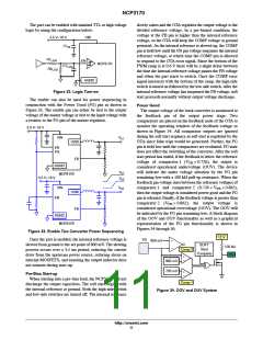
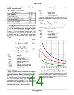
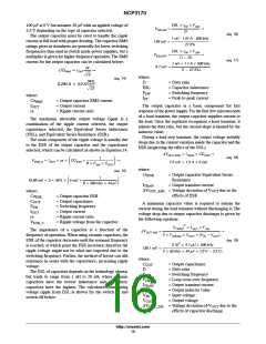
Light Load Operation
Light load operation is generally a load that is 1 mA to
300 mA where a load is in standby mode and requires very
little power. During light load operation, the regulator
emulates the operation of a non-synchronous buck converter
and the regulator is allowed to skip pulses. The
non-synchronous buck emulation is accomplished by
detecting the point at which the current flowing in the
inductor goes to zero and turning the low side switch off. At
the point when the current goes to zero, if the low side switch
is not turned off, current would reverse, discharging the
output capacitor. Since the low side switch is shutoff, the
only conduction path is through the body diode of the low
side MOSFET, which is back biased. Unlike traditional
synchronous buck converters, the current in the inductor
will become discontinuous. As a result, the switch node will
oscillate with the parasitic inductances and capacitances
connected to the switch node. The OTA will continue to
regulate the output voltage, but will skip pulses based on the
output load shown in Figure 37.
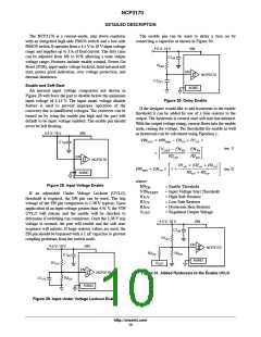
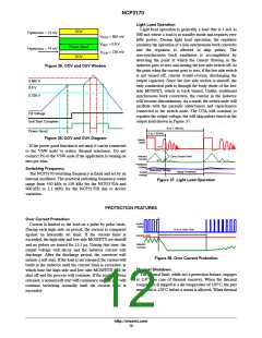
OOV
Hysteresis = 14 mV
Hysteresis = 14 mV
V
OOV
V
REF
V
OUV
= 862 mV
= 0.8 V
Power Good
OUV
= 726 mV
Figure 35. OOV and OUV Window
0.862 V
0.8 V
0.726 V
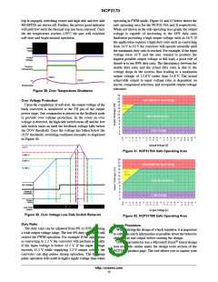
FB Voltage
Soft Start Complete
6 ms = 166 kHz
Power Good
2 ms = 50 kHz
Figure 36. OOV and OUV Diagram
Switch
Node
If the power good function is not used, it can be connected
to the VSW node to reduce thermal resistance. Do not
connect PG to the VSW node if the application is turning on
into pre-bias.
0V
Zero Current Point
Inductor
Current
0A
Feedback
Voltage
Switching Frequency
Reference Votlage
Ramp Threshold
COMP
Voltage
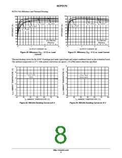
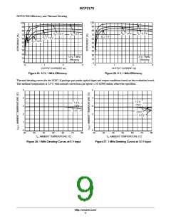
The NCP3170 switching frequency is fixed and set by an
internal oscillator. The practical switching frequency could
range from 450 kHz to 550 kHz for the NCP3170A and
900 kHz to 1.1 MHz for the NCP3170B due to device
variation.
Figure 37. Light Load Operation
PROTECTION FEATURES
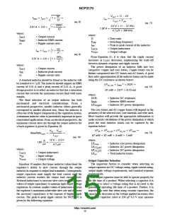
Over Current Protection
Switch
Current is limited to the load on a pulse by pulse basis.
During each high side on period, the current is compared
against an internally set limit. If the current limit is
exceeded, the high side and low side MOSFETS are shutoff
and no pulses are issued for 13.5 ms. During that time, the
output voltage will decay and the inductor current will
discharge. After the discharge period, the converter will
initiate a soft start. If the load is not released, the current will
build in the inductor until the current limit is exceeded, at
which time the high side and low side MOSFETS will be
shut off and the process will continue. If the load has been
released, a normal soft start will commence and the part will
continue switching normally until the current limit is
exceeded.
Node
13.5 ms Hold Time
Current Limit
Inductor
Current
Figure 38. Over Current Protection
Thermal Shutdown
The thermal limit, while not a protection feature, engages
at 150°C in case of thermal runaway. When the thermal
comparator is tripped at a die temperature of 150°C, the part
must cool to 120°C before a restart is allowed. When thermal
http://onsemi.com
12

 ONSEMI [ ONSEMI ]