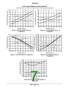
NCP3170
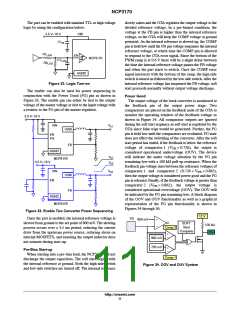
The part can be enabled with standard TTL or high voltage
logic by using the configuration below.
slowly raises and the OTA regulates the output voltage to the
divided reference voltage. In a pre-biased condition, the
voltage at the FB pin is higher than the internal reference
voltage, so the OTA will keep the COMP voltage at ground
potential. As the internal reference is slewed up, the COMP
pin is held low until the FB pin voltage surpasses the internal
reference voltage, at which time the COMP pin is allowed
to respond to the OTA error signal. Since the bottom of the
PWM ramp is at 0.6 V there will be a slight delay between
the time the internal reference voltage passes the FB voltage
and when the part starts to switch. Once the COMP error
signal intersects with the bottom of the ramp, the high side
switch is turned on followed by the low side switch. After the
internal reference voltage has surpassed the FB voltage, soft
start proceeds normally without output voltage discharge.
4.5 V−18 V
VIN
C1
IN
R1
LOG
EN
NCP3170
C1
LOG
R2
LOG
AGND
Figure 32. Logic Turn-on
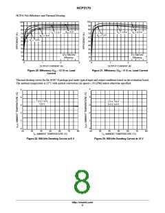
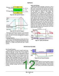
The enable can also be used for power sequencing in
conjunction with the Power Good (PG) pin as shown in
Figure 33. The enable pin can either be tied to the output
voltage of the master voltage or tied to the input voltage with
a resistor to the PG pin of the master regulator.
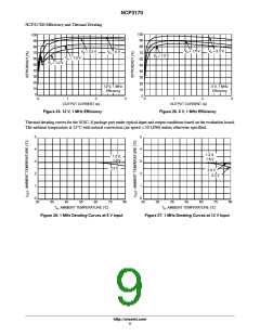
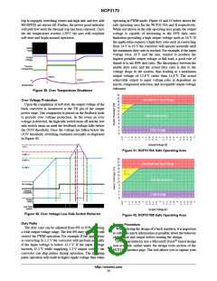
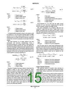
Power Good
The output voltage of the buck converter is monitored at
the feedback pin of the output power stage. Two
comparators are placed on the feedback node of the OTA to
monitor the operating window of the feedback voltage as
shown in Figure 34. All comparator outputs are ignored
during the soft start sequence as soft start is regulated by the
OTA since false trips would be generated. Further, the PG
pin is held low until the comparators are evaluated. PG state
does not affect the switching of the converter. After the soft
start period has ended, if the feedback is below the reference
4.5 V−18 V
V
o1
VIN
EN
VSW
FB
PG
voltage of comparator 1 (V < 0.726), the output is
FB
AGND
considered operational undervoltage (OUV). The device
will indicate the under voltage situation by the PG pin
remaining low with a 100 kW pull-up resistance. When the
feedback pin voltage rises between the reference voltages of
V
o1
NCP3170
4.5 V−18 V
V
o2
V
VIN
EN
comparator 1 and comparator 2 (0.726 < V < 0.862),
then the output voltage is considered power good and the PG
pin is released. Finally, if the feedback voltage is greater than
o2
FB
VSW
FB
comparator 2 (V > 0.862), the output voltage is
FB
considered operational overvoltage (OOV). The OOV will
be indicated by the PG pin remaining low. A block diagram
of the OOV and OUV functionality as well as a graphical
representation of the PG pin functionality is shown in
Figures 34 through 36.
AGND
NCP3170
Figure 33. Enable Two Converter Power Sequencing
12 V
Once the part is enabled, the internal reference voltage is
slewed from ground to the set point of 800 mV. The slewing
process occurs over a 4.5 ms period, reducing the current
draw from the upstream power source, reducing stress on
internal MOSFETS, and ensuring the output inductor does
not saturate during start-up.
FB
800 mV
+
SOFT
Start
Complete
100 kW
−
Comp 2
PG
+
−
862 mV
726 mV
+
−
Pre-Bias Start-up
When starting into a pre-bias load, the NCP3170 will not
discharge the output capacitors. The soft start begins with
the internal reference at ground. Both the high side switch
and low side switches are turned off. The internal reference
Comp 1
Figure 34. OOV and OUV System
http://onsemi.com
11

 ONSEMI [ ONSEMI ]