NCP3170
DETAILED DESCRIPTION
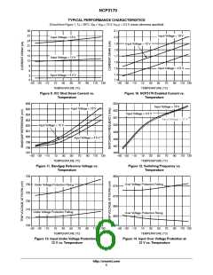
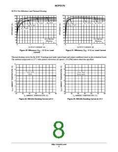
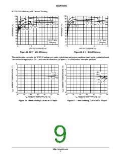
The NCP3170 is a current-mode, step down regulator
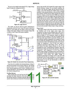
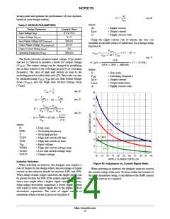
The enable pin can be used to delay a turn on by
connecting a capacitor as shown in Figure 30.
with an integrated high-side PMOS switch and a low-side
NMOS switch. It operates from a 4.5 V to 18 V input voltage
range and supplies up to 3 A of load current. The duty ratio
can be adjusted from 8% to 92% allowing a wide output
voltage range. Features include enable control, Power-On
Reset (POR), input under voltage lockout, fixed internal soft
start, power good indication, over voltage protection, and
thermal shutdown.
4.5 V−18 V
VIN
C1
IN
R
bias
EN
NCP3170
C1
DLY
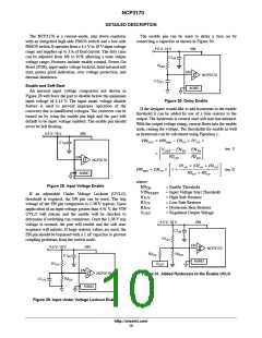
Enable and Soft-Start
AGND
An internal input voltage comparator not shown in
Figure 28 will force the part to disable below the minimum
input voltage of 4.13 V. The input under voltage disable
feature is used to prevent improper operation of the
converter due to insufficient voltages. The converter can be
turned on by tying the enable pin high and the part will
default to be input voltage enabled. The enable pin should
never be left floating.
Figure 30. Delay Enable
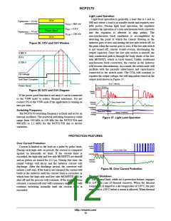
If the designer would like to add hysteresis to the enable
threshold it can be added by use of a bias resistor to the
output. The hysteresis is created once soft start has initiated.
With the output voltage rising, current flows into the enable
node, raising the voltage. The thresholds for enable as well
as hysteresis can be calculated using Equation 1.
4.5 V−18 V
VIN
VINHYS + VINStart * ENTH ) R1UV
C1
IN
(eq. 1)
VOUT * ENTH
ENTH
R2UV
ƪ
ƫ
*
R3UV
EN
NCP3170
ǒ
Ǔ
R1UV R2UV ) R3UV
(eq. 2)
VINStart + ENTH
ƪ
1 )
ƫ
R2UV R3UV
AGND
where:
Figure 28. Input Voltage Enable
EN
= Enable Threshold
TH
VIN
= Input Voltage Start Threshold
= High Side Resistor
= Low Side Resistor
= Hysteresis Bias Resistor
= Regulated Output Voltage
START
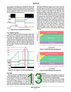
If an adjustable Under Voltage Lockout (UVLO)
threshold is required, the EN pin can be used. The trip
voltage of the EN pin comparator is 1.38 V typical. Upon
application of an input voltage greater than 4.41 V, the VIN
UVLO will release and the enable will be checked to
determine if switching can commence. Once the 1.38 V trip
voltage is crossed, the part will enable and the soft start
sequence will initiate. If large resistor values are used, the
EN pin should be bypassed with a 1 nF capacitor to prevent
coupling problems from the switch node.
R1
R2
R3
UV
UV
UV
V
OUT
4.5 V−18 V
C1
VIN
IN
R1
UV
EN
4.5 V−18 V
VIN
NCP3170
R2
R3
UV
UV
C1
IN
AGND
R1
V
OUT
UV
EN
NCP3170
Figure 31. Added Hysteresis to the Enable UVLO
R2
C1
UV
UV
AGND
Figure 29. Input Under Voltage Lockout Enable
http://onsemi.com
10

 ONSEMI [ ONSEMI ]