NCP1631
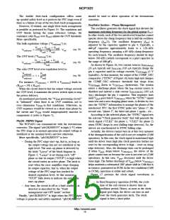
− However, the coil current can possibly be non
zero when the clock signal turns high. The
circuit would enter Continuous Conduction
current has totally vanished. In other words,
critical conduction mode (CrM) operation is
obtained.
Mode (CCM) if the MOSFET turned on in that
moment. In order to avoid CCM operation, the
clock is prevented from setting the PWM latch
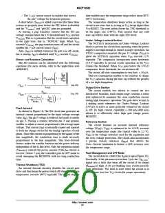
The clamp frequency can be computed using the
following equation:
60 m
COSC ) 10 p
(eq. 17)
fosc
^
until the core is reset (that is as low as “V
”
ZCD
of Figure 8 is low). The clock signal remains
high during this waiting phase (refer to
Figure 12). Hence the next MOSFET
conduction time occurs as soon as the coil
where C
is the pin 4 external capacitor and C the pin
pin
OSC
4 parasitic capacitance (about 10 pF).
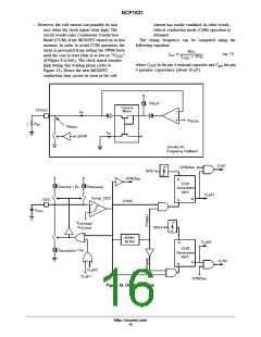
105 mA
Current
Mirror
FFOLD
I
FF
V
REGUL
R
FF
V
REGUL
I
FF
pfcOK
Circuitry for
Frequency Foldback
CLK1
SYNCbar
DRV1
SYNCbar
R
CLK1
Generation
latch
I
= I
FF
I
OSC(CH)
OSC(clamp)
Q_ph1
Comp_OSC
Q
S
OSC
SYNC
C
OSC
V
/
OSC(high)
V
DRV2
OSC(low)
divider
by two
Q_ph2
R
CLK2
Generation
latch
I
= I
FF
OSC(DISCH)
CLK2
Q
S
Q_ph2
Q_ph1
SYNCbar
Figure 16. Oscillator Block
http://onsemi.com
16

 ONSEMI [ ONSEMI ]