NCP1631
− The 7−mA current source is enabled that lowers
then enabled once the temperature drops below about 80°C
the pin7 voltage for hysteresis purpose.
(60°C hysteresis).
A short delay (T
) is added to get sure that these three
The temperature shutdown keeps active as long as the
delay
actions are properly done before the PFC driver is disabled
and the “V ” and “pfcOK” pins are grounded.
circuit is not reset, that is, as long as V keeps higher than
CC
V RESET. The reset action forces the TSD threshold to
CC
control
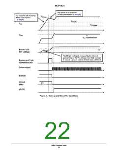
At startup, a pnp transistor ensures that the BO pin
voltage remains below the 1 V threshold until V reaches
be the upper one (140°C). This ensures that any cold
start−up will be done with the right TSD level.
CC
V
.This is to guarantee that the circuit starts operation
CC(on)
Under−Voltage Lockout Section
in the right state, that is, “BONOK” high. When V
exceeds V
enables the 7−mA current source (I ).
CC
The NCP1631 incorporates an Under−Voltage Lockout
block to prevent the circuit from operating when the power
supply is not high enough to ensure a proper operation. An
UVLO comparator monitors the pin 12 voltage (V ) to
allow the NCP1631 operation when V
, the pnp transistor turns off and the circuit
CC(on)
BO
Also, (I ) is enabled whenever the part is in off−mode,
BO
CC
but at startup, I is disabled until V reaches V .
BO
CC
CC(on)
exceeds 12 V
CC
typically. The comparator incorporates some hysteresis
Brown−out Resistors Calculation
The BO resistors can be calculated with the following
equations (for more details, refer to the application note
AND8407)
(2.0 V typically) to prevent erratic operation as the V
CC
crosses the threshold. When V goes below the UVLO
CC
comparator lower threshold, the circuit turns off.
The circuit off state consumption is very low: < 50 mA.
This low consumption enables to use resistors to charge
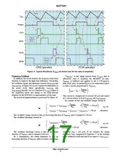
fline
ȡ
ȣ
10 ȣ
ȡ
1 *
boL
Ȣ
(Vin,avg
)
boH * (V
)
the V capacitor during the start−up without the penalty
ȧ
ȧ
ȧȧ
in,avg
CC
3fline
of a too high dissipation.
Ȥ
Ȥ
Ȣ
(eq. 23)
(eq. 24)
Rbo1
+
+
IHYST
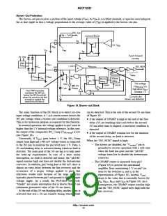
Output Drive Section
The circuit embeds two drivers to control the two
interleaved branches. Each output stage contains a totem
pole optimized to minimize the cross conduction current
during high frequency operation. The gate drive is kept in
a sinking mode whenever the Under−Voltage Lockout
(UVLO) is active or more generally whenever the circuit
is off. Its high current capability (−500 mA/+800 mA)
allows it to effectively drive high gate charge power
MOSFET.
Rbo1
Rbo2
(Vin,avg
)
fBO
3fline
boL
ǒ1 * Ǔ
ǒ
Ǔ
* 1
VBO(th)
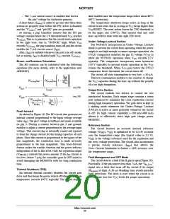
Feed−forward
As shown by Figure 19, The BO circuit also generates an
internal current proportional to the input voltage average
value (I ). The pin7 voltage is buffered and made available
Rt
on pin 3. Placing a resistor between pin 3 and ground,
enables to adjust a current proportional to the average input
Reference Section
The circuit features an accurate internal reference
voltage. This current (I ) is internally copied and squared
Rt
voltage (V ). V
is optimized to be 2.4% accurate
REF
REF
to form the charge current for the timing capacitor of each
phase. Since this current is proportional to the square of the
line magnitude, the conduction time is made inversely
proportional to the line magnitude. This feed−forward
feature makes the transfer function and the power delivery
independent of the ac line level. Only the regulation output
over the temperature range (the typical value is 2.5 V).
is the voltage reference used for the regulation and
the over−voltage protection. The circuit also incorporates
V
REF
a precise current reference (I ) that allows the
REF
Over−Current Limitation to feature a 6% accuracy over
the temperature range.
(V
) controls the power amount. If the I current is
REGUL
Rt
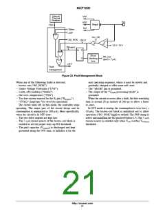
Fault Management and OFF Mode
too low ( below 7 mA), the controller goes in OFF mode to
avoid damaging the MOSFETs with too long conduction
time.
The circuit detects a fault if the R pin is open (Figure 20).
t
Practically, if the pin sources less than 7 mA, the “I
signal sets a latch that turns off the circuit if its output
”
Rt_Low
Thermal Shutdown (TSD)
(R ) is high. A 30−ms blanking time avoids parasitic
t(open)
An internal thermal circuitry disables the circuit gate
drive and then keeps the power switch off when the junction
temperature exceeds 140°C typically. The output stage is
fault detections. The latch is reset when the circuit is in
UVLO state (too low V levels for proper operation).
CC
http://onsemi.com
20

 ONSEMI [ ONSEMI ]