NCP1631
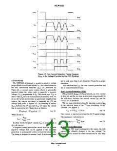
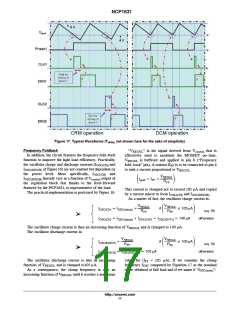
Figure 17. Typical Waveforms (Tdelay not shown here for the sake of simplicity)
Frequency Foldback
“V
” is the signal derived from V
that is
REGUL
control
In addition, the circuit features the frequency fold−back
function to improve the light load efficiency. Practically,
effectively used to modulate the MOSFET on−time.
V
REGUL
is buffered and applied to pin 6 (“Frequency
the oscillator charge and discharge currents (I
and
fold−back” pin). A resistor R is to be connected to pin 6
OSC(CH)
FF
I
of Figure16) are not constant but dependent on
to sink a current proportional to V
OSC(DISCH)
REGUL
the power level. More specifically,
linearly vary as a function of V
I
and
output of
OSC(CH)
VREGUL
RFF
I
ǒI
Ǔ.
pin6 + IFF
+
OSC(DISCH)
control
the regulation block that thanks to the feed−forward
featured by the NCP1631, is representative of the load.
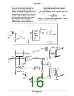
The practical implementation is portrayed by Figure 16.
This current is clamped not to exceed 105 mA and copied
by a current mirror to form I and I
.
OSC(DISCH)
OSC(CH)
As a matter of fact, the oscillator charge current is:
VREGUL
RFF
VREGUL
RFF
if ǒ v 105 mAǓ
IOSC(CH) + IOSC(clamp)
)
(eq. 18)
IOSC(CH) + IOSC(clamp) ) IOSC(CH1) + IOSC(CHT1) + 140 mA
otherwise
The oscillator charge current is then an increasing function of V
The oscillator discharge current is:
and is clamped to 140 mA.
REGUL
VREGUL
VREGUL
RFF
if ǒ v 105 mAǓ
IOSC(DISCH)
+
RFF
IOSC(DISCH) + IOSC(DISCH1) + 105 mA
(eq. 19)
otherwise
The oscillator discharge current is also an increasing
function of V and is clamped to105 mA.
value for (I = 105 mA). If we consider the clamp
FF
frequency f
computed by Equation 17 as the nominal
REGUL
OSC
As a consequence, the clamp frequency is also an
increasing function of V until it reaches a maximum
value obtained at full load and if we name it “f
”:
OSC(nom)
REGUL
http://onsemi.com
17

 ONSEMI [ ONSEMI ]