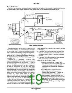
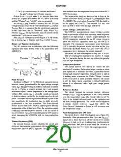
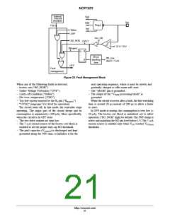
NCP1631
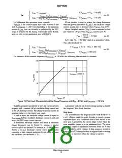
Brown−Out Protection
The brown−out pin receives a portion of the input voltage (V ). As V is a rectified sinusoid, a capacitor must integrate
IN
IN
the ac line ripple so that a voltage proportional to the average value of (V ) is applied to the brown−out pin.
IN
IRt_low
I
Rt
< 7 mA
Current Mirror
Rt
I
Rt
V
BO
R
Rt
V
in
V
BO
I
Rt
Feed−forward
Ac line
circuitry
EMI
Filter
R
bo1
V
1 V
s
C
in
BOcomp
BO_NOK
BO
s
1
T
delay
R
CS
R
bo2
S
C
bo
50-ms
deꢀlaꢀy
2
50-ms
deꢀlꢀaꢀy
Q
L
BO
R
This voltage
Vdd
7 mA
res et
reset
980 mV
Claꢀmp
(“V ”) is
BOcomp
high when V
pin7
This PNP transistor
is below 1 V
maintains the BO pin
below the BO threshold
when the circuit is not fed
enough to control the
stateof theBOblock
Circuitry for
brown−out detection
Figure 19. Brown−out Block
The main function of the BO block is to detect too low
input voltage conditions. A 7−mA current source lowers the
BO pin voltage when a brown−out condition is detected.
This is for hysteresis purpose as required by this function.
In nominal operation, the voltage applied to pin7 must be
higher than the 1 V internal voltage reference. In this case,
can be detected. This is the role of the second 50−ms timer
of Figure 19:
• if the output of OPAMP is high at the end of the first
delay (50−ms blanking time) and before the second
50−ms delay time is elapsed, a brownout condition is
detected
• if the output of OPAMP remains low for the duration
of the second delay, no fault is detected.
the output of the comparator BO_Comp (V
(see Figure 19).
) is low
BOcomp
Conversely, if V
goes below 1 V, the BO_Comp
pin7
When the “BO_NOK” signal is high:
output turns high and a 965 mV voltage source is connected
to the BO pin to maintain the pin level near 1 V. Then, a
50−ms blanking delay is activated during which no fault is
detected. The main goal of the 50−ms lag is to help meet
the hold−up requirements. In case of a short mains
interruption, no fault is detected and hence, the “pfcOK”
signal remains high and does not disable the downstream
converter. In addition, pin7 being kept at 965 mV, there is
almost no extra delay between the line recovery and the
occurrence of a proper voltage applied to pin2, that
otherwise would exist because of the large capacitor
typically placed between pin7 and ground to filter the input
voltage ripple. As a result, the NCP1631 effectively
“blanks” any mains interruption that is shorter than 25 ms
(minimum guaranteed value of the 50−ms timer).
− The drivers are disabled, the “V
” pin is
control
grounded to recover operation with a soft−start
when the fault has gone and the “pfcOK”
voltage turns low to disable the downstream
converter.
− The OPAMP output is separated from pin7
(Figure 19) to prevent the operational
amplifier from maintaining 1 V on pin7 (as
done by the switches s and s in the
1
2
representation of Figure 19). Instead, V
pin2
drops to the value that is externally forced (by
V , R , R and C in Figure 19). As a
in
bo1
bo2
bo2
consequence, the OPAMP output remains high
and the “BO_NOK” signal stays high until the
line recovers.
At the end of this 50−ms blanking delay, another timer is
activated that sets a 50−ms window during which a fault
http://onsemi.com
19

 ONSEMI [ ONSEMI ]