NCP1631
ǒ
@ 105 mAǓ
fOSC + fOSC(nom)
REGUL(RFF OSC(clamp)
60 m RFF(RFF OSC(clamp)
if VREGUL w RFF
(eq. 20)
V
I
) VREGUL
)
ǒ
@ 105 mAǓ
fOSC
+
@ fOSC(nom)
if VREGUL v RFF
I
) 2VREGUL
)
Let’s illustrate this operation on an example.
is the control signal that varies between 0 and
If one decides to start to reduce the clamp frequency
when the power goes below (P ) /2, the oscillator charge
V
REGUL
in HL
1.66 V, (V
= 1.66 V) corresponding to the maximum
current should start to decrease when V
is 0.83 V.
REGUL
REGUL
power (P ) that can virtually be delivered by the PFC
Hence, the pin 6 resistor (“R ”) must be selected so that
in HL
FF
stage as selected by the timing resistor (for more details,
you can refer to the application note AND8407).
pin 6 sources 105 mA when V
equates 0.83 V:
REGUL
0.83 V
RFF
+
+ 7.9 kW
(eq. 21)
105 mA
Let’s take (R = 8.2 kW) which is a normalized value.
FF
This selection leads to:
ǒ w 8.2 k @ 105 m + 860 mVǓ
if VREGUL
fOSC + fOSC(nom)
(eq. 22)
V
REGUL(RFFIOSC(clamp) ) VREGUL)
ǒ
v 860 mVǓ
fOSC
+
@ fOSC(nom)
if VREGUL
492 m(RFF OSC(clamp)
I
) 2VREGUL
)
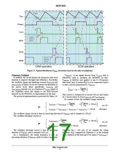
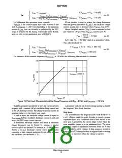
For instance, if the nominal frequency (f ) is 120 kHz, the following characteristic is obtained.
OSC(nom)
150
100
50
f
= 120 kHz
OSC(nom)
0
0
0.5
1
1.5
V
(V)
REGUL
Figure 18. Fold−back Characteristic of the Clamp Frequency with RFF = 8.2 kW and fOSC(nom) = 120 kHz
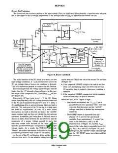
If pin6 is grounded (accidently or not), the circuit operates
properly with a constant 140 mA oscillator charge current and
a 105 mA discharge current. The clamp frequency equates its
nominal value over the whole load range.
A transistor pulls the pin 6 down during startup to disable
the frequency fold−back function.
Skip Mode
The circuit features the frequency fold−back that leads to
a very efficient stand−by mode. In order to ensure a proper
regulation in no load conditions even if this feature is not
used (pin 6 grounded), the circuit skips cycles when the
error amplifier output is at its minimum level. The error
amplifier output is maintained between about 0.6 V and
3.6 V thanks to active clamps. A skip sequence occurs as
long as the 0.6 V clamp circuitry is triggered and switching
operation is recovered when the clamp is inactive.
If pin6 is open, the oscillator charge current is equal to
I
but the oscillator discharge current is null and
OSC(clamp)
hence the PFC stage cannot operate.
A minimum discharge current and hence a minimum
clamp frequency can be forced by placing a resistor
between pin 4 and ground. For instance, a 1.5−MW resistor
forces a 3.3−mA discharge current when the oscillator
capacitor is fully charged and about 2.6 mA when it is near
the oscillator low threshold (4 V).
http://onsemi.com
18

 ONSEMI [ ONSEMI ]