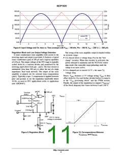
NCP1631
depending on the presence or absence of an effective
MOSFETs from the possible excessive stress it could suffer
from if it was allowed to turn on while a huge current
flowed through the coil as it can be the case at start−up or
during an over−load transient.
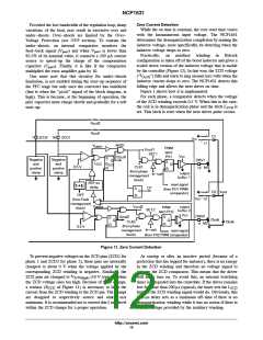
in−rush limiting circuitry. If the MOSFET turns on during
this severe transient, it may be over−stressed and finally
damaged. That is why, the NCP1631 permanently monitors
the input current and delays the MOSFET turn on until the
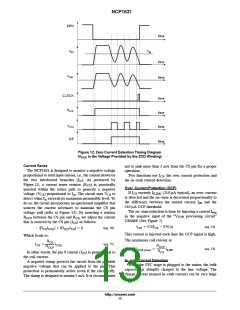
The propagation delay (I < I
) to (drive outputs
CS
in−rush
in−rush current has vanished. This is the function of the I
high) is in the range of few ms.
CS
comparison to the I
threshold (14 mA typical). When
, the comparator output (“In−rush”) is
However when the circuit starts to operate, the NCP1631
disables this protection to avoid that the current produced
by one phase and sensed by the circuit prevents the other
branch from operating. Practically, some logic grounds the
In−rush protection output when it detects the presence of
current cycles with a zero current detection signal provided
by the auxiliary winding (Figure 13).
in−rush
I
exceeds I
CS
in−rush
high and prevents the PWM latches from setting (see block
diagram). Hence, the two drivers cannot turn high and the
MOSFETs cannot switch on. This is to guarantee that the
MOSFETs remain off as long as if the input current exceeds
10% of its maximum value. This feature protects the
V
aux2
V
IN
I
V
OUT
D
2
IN
EMI
Filter
L
V
aux1
2
D
1
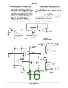
Current
Mirror
I
OCP
CS
C
IN
L
1
I
= 210 mA
ILIM1
M
2
The pin voltage
is maintained
I
CS
(I is proportional to the coil current)
CS
CS
DRV2
I
(from ZCD
block)
to 0 V
M
1
I
CS
CS
In−rush
Q
Q
ZCD1
DRV1
9
C
BULK
I
CS
ZCD2
I
= 14 mA
Negative clamp
in−rush
DRV1
DRV2
R
OCP
R
CS
I
IN
The CS block performs the over−current protection and the in−rush current detection.
Figure 13. Current Sense Block
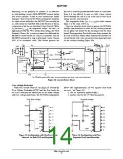
Over−Voltage Protection
While PFC circuits often use one single pin for both the
Over−Voltage Protection (OVP) and the feed−back, the
NCP1631 dedicates one specific pin for the under−voltage
and over−voltage protections. The NCP1631 configuration
allows the implementation of two separate feed−back
networks (see Figure 15):
1. One for regulation applied to pin 2.
2. Another one for the OVP function (pin 8).
Vout (bulk voltage)
Vout (bulk voltage)
Rout1
Rout1
16
15
1
2
16
15
14
1
FB
FB
2
3
3
4
14
13
12
11
10
9
Rout3
Rout2
Rovp1
Rovp2
Rout2
4
13
12
11
10
9
5
6
7
5
6
7
OVP
OVP
8
8
Figure 14. Configuration with One Feed−back
Figure 15. Configuration with Two
Network for Both OVP and Regulation
Separate Feed−back Networks
http://onsemi.com
14

 ONSEMI [ ONSEMI ]