NCP1631
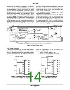
Zero Current Detection
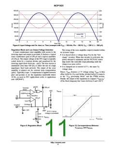
Provided the low bandwidth of the regulation loop, sharp
variations of the load, may result in excessive over and
under−shoots. Over−shoots are limited by the Over−
Voltage Protection (see OVP section). To contain the
under−shoots, an internal comparator monitors the
While the on time is constant, the core reset time varies
with the instantaneous input voltage. The NCP1631
determines the demagnetization completion by sensing the
inductor voltage, more specifically, by detecting when the
inductor voltage drops to zero.
feed−back signal (V ) and when V
is lower than
pin2
pin2
Practically, an auxiliary winding in flyback
configuration is taken off of the boost inductor and gives a
scaled down version of the inductor voltage that is usable
by the controller (Figure 12). In that way, the ZCD voltage
95.5% of its nominal value, it connects a 230 mA current
source to speed−up the charge of the compensation
capacitor (C ). Finally, it is like if the comparator
pin5
multiplied the error amplifier gain by 10.
(“V
”) falls and starts to ring around zero volts when the
One must note that this circuitry for under−shoots
limitation, is not enabled during the start−up sequence of
the PFC stage but only once the converter has stabilized
(that is when the “pfcOK” signal of the block diagram, is
high). This is because, at the beginning of operation, the
pin5 capacitor must charge slowly and gradually for a soft
start−up.
AUX
inductor current drops to zero. The NCP1631 detects this
falling edge and allows the next driver on time.
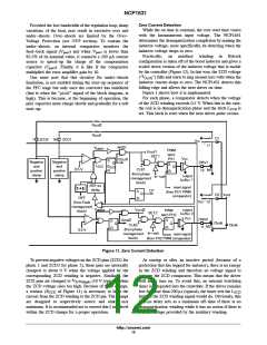
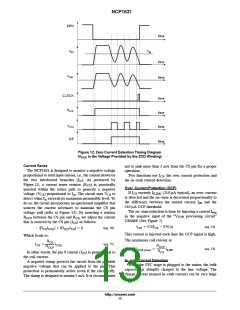
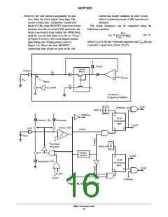
Figure 1 shows how it is implemented.
For each phase, a comparator detects when the voltage
of the ZCD winding exceeds 0.5 V. When this is the case,
the coil is in demagnetization phase and the latch L
is
ZCD
set. This latch is reset when the next driver pulse occurs.
Rzcd2
Rzcd1
D1
1
ZCD1
ZCD2 16
Vin
L1
AND1
V
DMG1
PWM
latch
PH1
Vzcd1
SET1
+
Vcc
Qzcd1
S
−
Negative
and
positive
Negative
and
positive
DRV1
Q
S
L
ZCD
Q
Q
ZCD
0.5 V
CLK1
(from phase
management
block)
M1
14
R
R
clamp
clamp
output
buffer 1
In−rush
200−ms
delay
reset signal
(from PH1 PWM
comparator)
DT
S
R
Q
Vout
D2
OFF
L2
Vin
(from Fault
management
V
DMG2
output
Vzcd2
PWM
latch PH2
block)
SET2
buffer 2
Vcc
+
−
DRV2
M2
Qzcd2
CLK2
(from phase
management
block)
S
S
R
Cbulk
Q
Q
Cbulk
11
R
0.5 V
In−rush
reset signal
(from PH2 PWM comparator)
Figure 11. Zero Current Detection
To prevent negative voltages on the ZCD pins (ZCD1 for
phase 1 and ZCD2 for phase 2), these pins are internally
clamped to about 0 V when the voltage applied by the
corresponding ZCD winding is negative. Similarly, the
At startup or after an inactive period (because of a
protection that has tripped for instance), there is no energy
in the ZCD winding and therefore no voltage signal to
activate the ZCD comparator. This means that the driver
will never turn on. To avoid this, an internal watchdog
timer is integrated into the controller. If the driver remains
ZCD pins are clamped to V
(10 V typical), when
ZCD(high)
the ZCD voltage rises too high. Because of these clamps,
a resistor (R of Figure 11) is necessary to limit the
low for more than 200 ms (typical), the timer sets the L
ZCD
ZCD
current from the ZCD winding to the ZCD pin. The clamps
are designed to respectively source and sink 5 mA
minimum. It is recommended not to exceed this 5 mA level
within the ZCD clamps for a proper operation.
latch as the ZCD winding signal would do. Obviously, this
200−ms delay acts as a minimum off−time if there is no
demagnetization winding while it has no action if there is
a ZCD voltage provided by the auxiliary winding.
http://onsemi.com
12

 ONSEMI [ ONSEMI ]