NCP1631
The double feed−back configuration offers some
should be used to allow operation of the downstream
converter.
up−graded safety level as it protects the PFC stage even if
there is a failure of one of the two feed−back arrangements.
However, if wished, one single feed−back arrangement
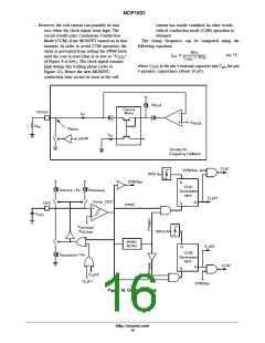
is possible as portrayed by Figure 14. The regulation and
OVP blocks having the same reference voltage, the
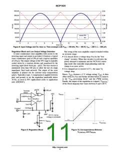
Oscillator Section – Phase Management
The oscillator generates the clock signal that dictates the
maximum switching frequency for the global system (f ).
osc
In other words, each of the two interleaved branches cannot
operate above the clamp frequency that is half the oscillator
resistance ratio R
over R
adjusts the OVP threshold.
out2
out3
More specifically,
frequency (f /2). The oscillator frequency (f ) is
osc
osc
The bulk regulation voltage (“V ”) is:
out(nom)
adjusted by the capacitor applied to pin 4. Typically, a
440 pF capacitor approximately leads to a 120−kHz
operating frequency, meaning a 60−kHz clamp frequency
for each branch. The oscillator frequency should be kept
below 500 kHz (which corresponds to a pin4 capacitor in
the range of 100 pF).
Rout1 ) Rout2 ) R
Rout2 ) Rout3
(eq. 14)
(eq. 15)
Vout(nom)
+
out3 @ Vref
The OVP level (“V ”) is:
out(ovp)
Rout1 ) Rout2 ) R
Vout(ovp)
+
out3 @ Vref
Rout2
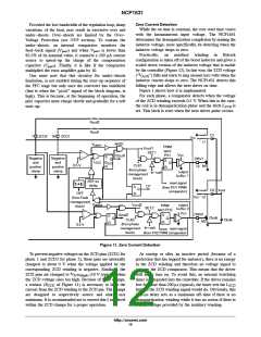
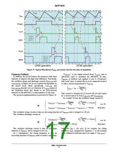
As shown by Figure 16, two current sources I
OSC(clamp)
(35 mA typical) and I
pin 4 capacitor until its voltage exceeds V
typically). At that moment, the output of the COMP_OSC
comparator (“SYNC” of Figure 16) turns high and changes
the COMP_OSC reference threshold that drops from
(105 mA typical) charge the
OSC(CH)
The ratio OVP level over regulation level is:
(5 V
OSC(high)
Vout(ovp)
Rout3
Rout2
(eq. 16)
+ 1 )
Vout(nom)
For instance, (V
= 105% x V
) leads to:
out(nom)
out(nom)
V
down to V
(hysteresis). The system
OSC(high)
OSC(low)
(R
= 5% x R ).
out3
out2
enters a discharge phase where the I current source is
disabled and instead a sink current I
CH
When the circuit detects that the output voltage exceeds
the OVP level, it maintains the power switch open to stop
the power delivery.
(105 mA
OSC(DISCH)
typ.) discharges the pin 4 capacitor. This sequence lasts
until V goes below V when the “SYNC” signal
pin4
OSC(low)
As mentioned previously, the “V
processing circuit”
TON
turns low and a new charging phase starts. A divider by two
uses the “SYNC” information to manage the phases of the
interleaved PFC: the first SYNC pulse sets “phase 1”, the
second one, “phase 2”, the third one phase 1 again... etc...
According to the selected phase, the “SYNC” signal sets
the relevant “Clock generator latch” that will generate the
clock signal (“CLK1” for phase 1, “CLK2” for phase 2)
when SYNC drops to zero (falling edge detector). So, the
drivers are synchronized to SYNC falling edge.
Actually, the drivers cannot turn on at this very moment
if the demagnetization of the coil is not yet complete (CrM
operation). In this case, the clock signal is maintained high
until the driver turns high (the clock generator latches are
reset by the corresponding driver is high − reset on rising
edge detector). Also, the discharge time can be prolonged
is “informed” when there is an OVP condition, not to
over−dimension V in that conditions. Otherwise, an
TON
OVP sequence would be viewed as a dead−time phase by
the circuit and V would inappropriately increase to
TON
compensate it (refer to Figure 7).
PfcOK / REF5V Signal
The NCP1631 can communicate with the downstream
converter. The signal “pfcOK/REF5V” is high (5 V) when
the PFC stage is in normal operation (its output voltage is
stabilized at the nominal level) and low otherwise.
More specifically, “pfcOK/REF5V” is low:
− During the PFC stage start−up, that is, as long as
the output voltage has not yet stabilized at the
right level. The start−up phase is detected by
if when V
drops below V
, the driver of the
OSC(low)
the latch “L ” of the block diagram in
STUP
pin4
phase cannot turn on because the core is not reset yet (CrM
operation). In this case, V decreases until the driver
Figure 2. “L
” is set during each “off”
STUP
phase so that its output (“STUP“) is high when
the circuit enters an active phase. The latch is
reset when the error amplifier stops charging
its output capacitor, that is, when the output
voltage of the PFC stage has reached its
desired regulation level. At that moment,
“STUP” falls down to indicate the end of the
start−up phase.
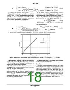
pin4
turns high. The further discharge of V
below V
pin4
OSC(low)
helps maintain a substantial 180° phase shift in CrM that is
in essence, guaranteed in DCM. In the two conditions (CrM
or DCM), operation is stable and robust.
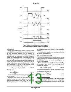
Figure 17 portrays the clock signal waveforms in
different cases:
− In fixed frequency operation (DCM), the cycle
time of the coil current is shorter than an
oscillator period. Hence, as soon as the clock
signal goes high, the driver can turn on and
reset the clock generator latch. The clock
signal is then a short pulse.
− Any time, the circuit is off or a fault condition is
detected as described by the “Fault
management and OFF mode” section
Finally, “pfcOK/REF5V” is high when the PFC output
voltage is properly and safely regulated. “pfcOK/REF5V”
http://onsemi.com
15

 ONSEMI [ ONSEMI ]