NCP1631
350,00
300,00
250,00
200,00
150,00
100,00
3,50
3,00
2,50
2,00
1,50
1,00
Vin
ton
50,00
0,00
0,50
0,00
0
2
4
6
8
10
time (ms)
12
14
16
18
20
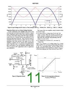
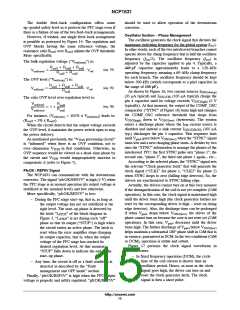
Figure 8. Input Voltage and On−time vs. Time (example with FSW = 100 kHz, Pin = 150 W, VAC = 230 V, L = 200 mH)
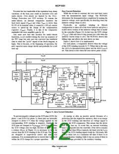
Regulation Block and Low Output Voltage Detection
A trans−conductance error amplifier with access to the
inverting input and output is provided. It features a typical
trans−conductance gain of 200 mS and a typical capability
of 20 mA. The output voltage of the PFC stage is typically
scaled down by a resistors divider and monitored by the
inverting input (feed−back pin – pin2). The bias current is
minimized (less than 500 nA) to allow the use of a high
impedance feed−back network. The output of the error
amplifier is pinned out for external loop compensation
(pin5). Typically a type−2 compensator is applied between
pin5 and ground, to set the regulation bandwidth below
20 Hz, as need in PFC applications (refer to application
note AND8407).
The swing of the error amplifier output is limited within
an accurate range:
• It is forced above a voltage drop (V ) by the “low
F
clamp” circuitry. When this circuitry is activated, the
power demand is minimum and the NCP1631 enters
skip mode (the controller stops pulsating) until the
clamp is no more active.
• It is clamped not to exceed 3.0 V + the same V
F
voltage drop.
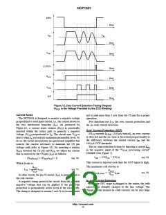
Hence, V
features a 3 V voltage swing. V
is then
pin5
pin5
offset down by (V ) and further divided before it connects
F
to the “V
processing block” and the PWM section.
ton
Finally, the output of the regulation is a signal (“V
”
REGUL
of the block diagram) that varies between 0 and 1.66 V.
pfcOK
230 mA
VDD
Vout low
detect
−
+
0.955*Vref
Error Amplifier
FB
−
20 mA
+
Vref
OVLflag1
Vcontrol
OFF
SKIP
(0.6 V clamp
voltage is activated)
5R
4R
V
REGUL
3V
Figure 9. Regulation Block
Figure 10. Correspondence Between
VCONTROL and VREGUL
http://onsemi.com
11

 ONSEMI [ ONSEMI ]