NCP1399AA, NCP1399BA, NCP1399AC
restart in such cases. The controller blanks the SKIP/REM
input information and pulls down the SKIP/REM input for
time during controller restart so that the
secondary side bias can be restored and the secondary
off−mode controller can activate the REM optocoupler. This
REM TIMER blank sequence is activated each time the
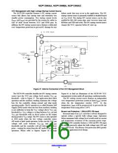
The bias on VCC pin needs to be assured when off−mode
operation takes place. The auxiliary winding is no more able
to provide any bias thus the HV startup current source is
operated in DSS mode – i.e. the VCC pin voltage is cycling
t
REM_TIMER
between V
and V
thresholds. This approach
CC_ON
CC_OFF
keeps IC biasing in order to memorize the current operation
sate.
VCC pin voltage reaches V
threshold – except in the
CC_ON
situation when after IC left off−mode operation by standard
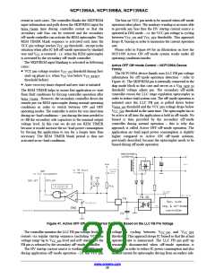
Please refer to Figure 64 for an illustration on how the
NCP1399 Active ON off−mode system works under all
operating conditions/modes.
way and V is restored – i.e. when the REM optocoupler
CC
is activated by the secondary off−mode controller.
The SKIP/REM input blanking is activated in following
cases:
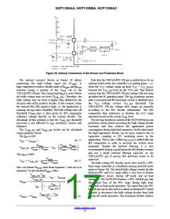
Active OFF Off−mode Control – NCP1399A Device
Family
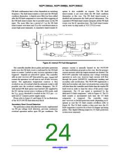
The NCP1399A device family uses LLC FB pin voltage
information for off−mode operation detection − refer to
Figure 41. The SKIP/REM pin is internally connected to the
• VCC pin voltage reaches V
threshold during first
CC_ON
start−up phase (i.e. when V was below V
CC
CC_RESET
threshold before)
• Auto−recovery timer elapsed and new start is initiated
skip mode block in this case and serves as a V
FB_SKIP_IN
threshold voltage adjust pin. The secondary off−mode
controller reuses the LLC stage regulation optocoupler in
order to reduce total system cost. The off−mode operation is
initiated once the LLC FB pin is pulled down below
The REM TIMER helps to assure fast application re−start
from fault conditions by forcing controller operation after
t
. However, the secondary controller drives the
REM_TIMER
remote pin via REM optocoupler during normal operating
conditions in order to switch between ON and OFF
operating modes. The controller is active for very short time
during no−load conditions − just during the time needed to
re−fill the secondary side capacitors to the nominal output
voltage level. In this case we do not use REM TIMER
because it would increase the no−load power consumption
by forcing the application to run for a longer time than
necessary. The REM TIMER blank period is thus not
activated in no−load conditions.
V
V
threshold and the VCC pin voltage drops below
threshold in the same time. The optocoupler has to
REM_ON
CC_OFF
be active at all time the application is held in off−mode. No
biased is then provided by the secondary off−mode
controller during normal operation – this is why this
approach is called Active OFF off−mode operation. The
application no−load input power consumption is slightly
higher compared to Active ON off−mode solution,
previously described, because the optocoupler needs to be
biased during off mode operation
Figure 41. Active OFF Off−mode Internal Detection Based on the LLC FB Pin Voltage
The controller monitors the LLC FB pin voltage level and
restarts via regular startup sequence (including VCC pin
voltage is cycling between V
and V
CC_ON CC_OFF
thresholds. This approach keeps IC biased so that the actual
operation sate is memorized. The LLC FB pin pull−up
resistor is disconnected when off−mode operation is
activated in order to reduce IC power consumption and also
needed current for optocoupler driving from secondary side.
voltage ramp−up to V
level and soft−start) once the
CC_ON
FB pin is released by the secondary off−mode controller.
The HV startup current source is working in DSS mode
during application off−mode operation – i.e. the VCC pin
www.onsemi.com
20

 ONSEMI [ ONSEMI ]