NCP1399AA, NCP1399BA, NCP1399AC
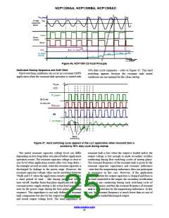
Please refer to Figure 65 for an illustration on how the
NCP1399 active ON off−mode system works under all
operating conditions/modes.
P ON/OFF pin is 1 kW. The PFC stage operation can thus be
disabled/enabled via external logic signal. This option
should be used with the wide range input voltage LLC tank
designed to assure correct operation of the LLC stage
through whole bulk voltage range. The PFC MODE output
pin can be used for two purposes:
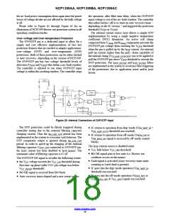
PFC MODE Output and P ON/OFF Control Pin
The NCP1399 has two pins P ON/OFF and PFC MODE
that can be used to disable or enable PFC stage operation
based on actual application operating state – please refer to
Figure 46. The PFC MODE pin voltage is changed
1. to control the external small signal HV MOSFET
switch that connects the bulk voltage divider to the
VBULK/PFC FB input
2. to control the PFC front stage controller operation
via PFC controller supply pin
(V
or V
) based on the actual P ON/OFF
PFC_M_ON
PFC_M_BO
input logic signal state. Minimum impedance connected to
5 V
0.1 V
Figure 42. Internal Connection of the PFC MODE and P ON/OFF Blocks
There are three possible states of the PFC MODE output
that can be placed by the controller based on the application
operating conditions:
connects VCC pin voltage to PFC MODE output
with minimum dropout (V ). This state of
the PFC MODE output appears in case an external
signal on the P ON/OFF pin is at “low” state.
PFC_M_ON
1. The PFC MODE output pin is pulled−down by an
internal MOSFET switch before controller startup.
This technique ensures minimum VCC pin current
The output power level is derived internally from the
actual FB pin voltage. This information could be compared
on external comparator with the reference level and control
the P ON/OFF input, thus the user has possibility to adjust
power below which the PFC stage is disabled in order to
increase efficiency in light load conditions. The P ON/OFF
consumption in order to ramp V voltage in a
CC
short time from the HV startup current source
which speeds up the startup or restart process. The
PFC MODE output pin is also pulled−down in
off−mode or protection mode during which the HV
startup current source is operated in DSS mode.
This reduces the application power consumption in
both cases.
comparator features an hysteresis (P ON/OFF
)
HYST
proportional to the set P ON/OFF level in order to overcome
PFC power stage oscillations (periodical ON/OFF
2. The pull−down switch is disabled and the internal
regulator enabled by the controller to provide
operation). The P ON/OFF timer (t
) is
P ON/OFF_TIMER
implemented to ensure a long enough propagation delay
from the PFC turn OFF detection to PFC MODE output
deactivation. This timer is unidirectional so that it resets
immediately after PFC ON condition is detected by the
P ON/OFF comparator. This technique is used in order to
avoid a PFC stage deactivation during load or line transients.
The PFC MODE pin output current is limited when the VCC
to PFC MODE bypass switch is activated. The current
limitation avoids bypass switch damage during PFC VCC
decoupling capacitor charging process or short circuit. A
minimum value PFC VCC decoupling capacitance should
be used in order to speed up PFC stage startup after it is
enabled by the NCP1399 controller.
V
reference when an external logic
PFC_M_BO
signal on the P ON/OFF pin is at “high” state. An
internal regulator includes current limitation for
the PFC MODE output that is set to I
PFC_M_LIM
when V
reference is provided. The PFC
PFC_M_BO
MODE pin drives external small signal HV
MOSFET switch to keep bulk voltage divider
connected. The LLC power stage Brown−out
protection system thus works when the LLC stage
is switching while PFC stage disabled.
3. The pull−down switch is disabled and the internal
regulator is switched to bypass mode in which it
www.onsemi.com
21

 ONSEMI [ ONSEMI ]