NCP1399AA, NCP1399BA, NCP1399AC
The second input signal for the on−time comparator is
passes through the FB processing block before it is brought
to the ON−time comparator input. The FB processing block
derived from the FB pin voltage. This internal FB pin signal
is also used for the following purposes: skip mode operation
detection, PFC MODE control, off−mode detection (in
NCP1399A device family) and overload / open FB pin fault
detection. The detailed description of these functions can be
found in each dedicated chapters. The internal pull−up
resistor assures that the FB pin voltage increases when the
optocoupler LED becomes less biased – i.e. when output
load is increased. The higher FB pin voltage implies a higher
reference level for on−time comparator i.e. longer Mupper
switch on−time and thus also higher output power. The FB
pin features a precise voltage clamp which limits the internal
FB signal during overload and startup. The FB pin signal
scales the FB signal down by a K ratio in order to limit the
FB
CS input dynamic voltage range. The scaled FB signal is
then further processed by subtraction of
a ramp
compensation generator signal in order to ensure stability of
the current mode control scheme. The divided internal FB
signal is overridden by a Soft−start generator output voltage
during device starts−up.
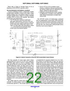
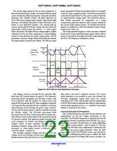
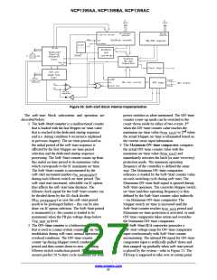
The actual operation frequency of the converter is defined
based on the CS pin and FB pin input signals. Please refer to
Figure 44 and below description for better understanding of
the NCP1399 frequency modulation system.
Figure 44. NCP1399 On−time Modulation Principle
The Mupper switch is activated by the controller after
dead−time (DT) period lapses in point A. The frequency
processing block increments the ON−time counter with
10 ns resolution until the internal CS signal crosses the
internal FB set point for the ON−time comparator in point B.
A DT period is then introduced by the controller to avoid any
shoot−through current through the power stage switches.
The DT period ends in point C and the controller activates
the Mlower switch. The ON−time processing block
decrements the ON_time counter down until it reaches zero.
The Mlower switch is then turned−OFF at point D and the
DT period is started. This approach results in perfect duty
cycle symmetry for Mlower and Mupper switches. The
Mupper switch on−time naturally increases and the
operating frequency drops when the FB pin voltage is
increased, i.e. when higher current is delivered by the
converter output – sequence E.
skip mode is not used or adjusted correctly. The current
mode operation is not possible in such case because the
ON−time comparator output stays active for several
switching cycles. Thus a special logic has been implemented
in NCP1399 in order to repeat the last valid on−time until the
current mode operation recovers – i.e. until the CS pin signal
balance is restored by the system.
Overload and Open FB Protections
The overload protection and open FB pin detection are
implemented via FB pin voltage monitoring in this
controller. The FB fault comparator is triggered once the FB
pin voltage reaches its maximum level and the V
FB_FAULT
threshold is exceeded. The fault timer or counter (depending
on IC option) is then enabled – refer to Figure 43. The time
period to the FB fault event confirmation is defined by the
preselected t
parameter when the fault
FB_FAULT_TIMER
timer option is used. The FB fault counter, once selected as
a FB fault confirmation period source, defines the fault
confirmation period via Mupper DRV pulses counting. The
The resonant capacitor voltage and thus also CS pin
voltage can be out of balance in some cases – this is the case
during transition from full load to no−load operation when
www.onsemi.com
23

 ONSEMI [ ONSEMI ]