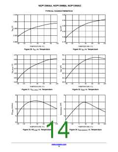
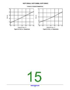
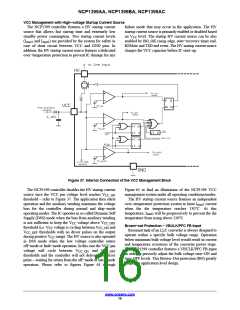
NCP1399AA, NCP1399BA, NCP1399AC
the no−load power consumption down again since the power
losses of voltage divider are not affected by the bulk voltage
at all.
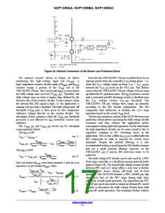
Please refer to Figure 61 through Figure 65 for an
illustration of NCP1399 Brown−out protection system in all
operating conditions/modes.
the operation, after filter time delay, when the OVP/OTP
input voltage is out of the no−fault window. The controller
then either latches−off or or starts an auto−recovery timer −
depending on the IC version − and triggered the protection
threshold (V
or V ).
OVP
OTP
The internal current source I
allows a simple OTP
OTP
implementation by using a single negative temperature
coefficient (NTC) thermistor. An active soft clamp
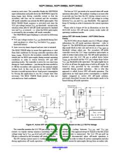
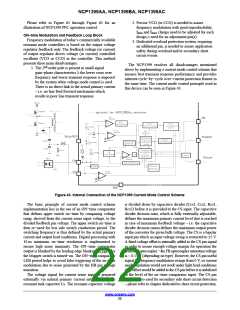
Over−voltage and Over−temperature Protection
The OVP/OTP pin is a dedicated input to allow for a
simple and cost effective implementation of two key
protection features that are needed in adapter applications:
over−voltage (OVP) and over−temperature (OTP)
protections. Both of these protections can be either latched
or auto−recovery– depending on the version of NCP1399.
The OVP/OTP pin has two voltage threshold levels of
composed from V
and R
components prevents the
clamp
clamp
OVP/OTP pin voltage from reaching the V
threshold
OVP
when the pin is pulled up by the I
current. An external
OTP
pull−up current, higher than the pull*down capability of
the internal clamp (V
pull the OVP/OTP pin above V
), has to be applied to
threshold to activate the
CLAMP_OVP/OTP
OVP
OVP protection. The t
and t
filters
OVP_FILTER
OTP_FILTER
detection (V
and V ) that define a no−fault window.
OTP
OVP
are implemented in the system to avoid any false triggering
of the protections due to application noise and/or poor
layout.
The controller is allowed to run when OVP/OTP input
voltage is within this working window. The controller stops
Figure 39. Internal Connection of OVP/OTP Input
The OTP protection could be falsely triggered during
controller startup due to the external filtering capacitor
• IC returns to operation from skip−mode (V
+
FB_SKIP_IN
V
threshold was reached)
FB_SKIP_HYST
charging current. Thus the t
period has been
BLANK_OTP
• IC returns to operation from off−mode (V
or
REM_ON
implemented in the system to overcome such behavior. The
OTP comparator output is ignored during t
V
signal is received by off−mode control
FB_REM_ON
BLANK_OTP
block)
period. In order to speed up the charging of the external
filtering capacitor C connected to OVP/OTP pin,
The I
current source is disabled when:
OTP
OVP_OTP
• V falls below V
threshold
CC
CC_OFF
the I
current has been doubled to I . The
OTP_BOOST
OTP
• BO OK signal goes to low state (i.e. Brown−out
condition occurs on the mains)
maximum value of filtering capacitor is 47 nF.
The OVP/OTP ON signal is set after the following events:
• the V voltage exceeds the V threshold during
• Fault signal is activated (Auto−recovery timer starts
counting or Latch fault is present)
CC
CC_ON
first start−up phase (after VCC pin voltage was below
threshold)
• IC goes into the skip−mode operation (V
V
FB_SKIP_IN
CC_RESET
threshold was reached)
• BO OK signal is received from BO block
• Auto−recovery timer elapsed and a new restart occurs
• IC goes into the off−mode operation (V
or
REM_OFF
) signal was reached)
(V
& V
FB_REM_OFF
CC_OFF
www.onsemi.com
18

 ONSEMI [ ONSEMI ]