NCP1399AA, NCP1399BA, NCP1399AC
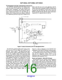
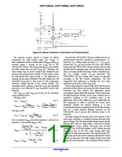
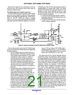
Figure 38. Internal Connection of the Brown−out Protection Block
The internal circuitry shown in Figure 38 allows
Note that the VBULK/PFC FB pin is pulled down by an
internal switch when the controller is in startup phase − i.e.
monitoring the high−voltage input rail (V ).
A
bulk
high−impedance resistive divider made of R
and R
when the V voltage ramps up from V < V
upper
lower
CC CC CC_RESET
resistors brings a portion of the V
rail to the
towards the V
level on the VCC pin. This feature
bulk
CC_ON
VBULK/PFC FB pin. The Current sink (I ) is active below
assures that the VBULK/PFC FB pin voltage will not ramp
BO
the bulk voltage turn−on level (V
). Therefore, the
up before the IC operation starts. The I hysteresis current
bulk_ON
BO
bulk voltage turn−on level is higher than defined by the
division ratio of the resistive divider. To the contrary, when
the internal BO_OK signal is high, i.e. the application is
sink is activated and BO discharge switch is disabled once
the
V
CC
voltage crosses
V
CC_ON
threshold. The
VBULK/PFC FB pin voltage then ramps up naturally
according to the BO divider information. The BO
comparator then authorizes or disables the LLC stage
running, the I sink is disabled. The bulk voltage turn−off
BO
threshold (V ) is then given by BO comparator
bulk_OFF
reference voltage directly on the resistor divider. The
advantage of this solution is that the V threshold
operation based on the actual V
level.
bulk
The low I hysteresis current of the NCP1399 brown out
bulk_OFF
BO
precision is not affected by I
tolerance.
hysteresis current sink
protection system allows increasing the bulk voltage divider
resistance and thus reduces the application power
consumption during light load operation. On the other hand,
the high impedance divider can be noise sensitive due to
capacitive coupling to HV switching traces in the
BO
The V
and V
levels can be calculated
bulk_ON
bulk_OFF
using equations below:
The I is ON:
BO
application. This is why a filter (t
) is added after the
BO_FILTR
(eq. 1)
VBO ) VBOhyst
+
BO comparator in order to increase the system noise
immunity. Despite the internal filtering, it is also
recommended to keep a good layout for BO divider resistors
and use a small external filtering capacitor on the
VBULK/PFC pin if precise BO detection wants to be
achieved.
The bulk voltage HV divider can be also used by a PFC
front stage controller as a feedback sensing network (refer
again to Figure 38). The shared bulk voltage resistor divider
between PFC and LLC stage offers a way how to further
reduce power losses during off−mode and no−load
operation. The NCP1399 features a PFC MODE pin that
disconnects bias of the PFC stage during light load,
off−mode or fault mode operation. The signal from the PFC
MODE pin can be also used to control an external HV switch
in order to disconnect the bulk voltage divider from bulk
during off−mode operation. This technique further reduces
Rlower
Rlower ) Rupper
Rlower @ Rupper
Rlower ) Rupper
@ ǒ
Ǔ
Vbulk_ON
@
* IBO
The I is OFF:
BO
Rlower
Rlower ) Rupper
VBO + Vbulk_OFF
@
(eq. 2)
One can extract R
term from equation 2 and use it in
lower
equation 1 to get needed R
value:
upper
Vbulk_ON@V
BO * VBO * VBOhyst
Vbulk_OFF
Rlower
+
(eq. 3)
(eq. 4)
VBO
IBO
@
ǒ
1 *
Ǔ
Vbulk_OFF
Vbulk_OFF * VBO
Rupper + Rlower
@
VBO
www.onsemi.com
17

 ONSEMI [ ONSEMI ]