NCP1399AA, NCP1399BA, NCP1399AC
VCC Management with High−voltage Startup Current Source
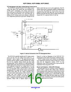
The NCP1399 controller features a HV startup current
source that allows fast startup time and extremely low
standby power consumption. Two startup current levels
failure mode that may occur in the application. The HV
startup current source is primarily enabled or disabled based
on V level. The startup HV current source can be also
CC
(I
and I
) are provided by the system for safety in
enabled by BO_OK rising edge, auto−recovery timer end,
REMote and TSD end event. The HV startup current source
charges the VCC capacitor before IC start−up.
start1
start2
case of short circuit between VCC and GND pins. In
addition, the HV startup current source features a dedicated
over−temperature protection to prevent IC damage for any
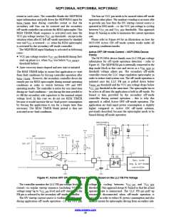
Figure 37. Internal Connection of the VCC Management Block
The NCP1399 controller disables the HV startup current
Figure 65 to find an illustration of the NCP1399 VCC
management system under all operating conditions/modes.
The HV startup current source features an independent
source once the VCC pin voltage level reaches V
CC_ON
threshold – refer to Figure 37. The application then starts
operation and the auxiliary winding maintains the voltage
bias for the controller during normal and skip−mode
operating modes. The IC operates in so called Dynamic Self
Supply (DSS) mode when the bias from auxiliary winding
over–temperature protection system to limit I
current
start2
when the die temperature reaches 130°C. At this
temperature, I will be progressively to prevent the die
start2
temperature from rising above 130°C.
is not sufficient to keep the V voltage above V
CC
CC_OFF
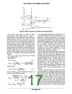
Brown−out Protection − VBULK/PFC FB Input
threshold (i.e. V voltage is cycling between V
and
CC
CC_ON
Resonant tank of an LLC converter is always designed to
operate within a specific bulk voltage range. Operation
below minimum bulk voltage level would result in current
and temperature overstress of the converter power stage.
The NCP1399 controller features a VBULK/PFC FB input
in order to precisely adjust the bulk voltage turn−ON and
turn−OFF levels. This Brown−Out protection (BO) greatly
simplifies application level design.
V
thresholds with no driver pulses on the output
CC_OFF
during positive V ramp). The HV source is also operated
in DSS mode when the low voltage controller enters
off−mode or fault−mode operation. In this case the VCC pin
CC
voltage will cycle between V
and V
CC_ON
CC_OFF
thresholds and the controller will not deliver any driver
pulse – waiting for return from the off−mode or latch mode
operation. Please refer to figures Figure 61 through
www.onsemi.com
16

 ONSEMI [ ONSEMI ]