NCP1399AA, NCP1399BA, NCP1399AC
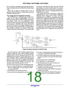
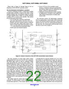
Please refer to Figure 61 through Figure 65 for an
illustration of NCP1399 PFC operation control.
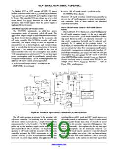
2. Precise VCO (or CCO) is needed to assure
frequency modulation with good reproducibility,
f
and f
clamps need to be adjusted for each
min
max
ON−time Modulation and Feedback Loop Block
Frequency modulation of today’s commercially available
resonant mode controllers is based on the output voltage
regulator feedback only. The feedback voltage (or current)
of output regulator drives voltage (or current) controlled
oscillator (VCO or CCO) in the controller. This method
presents three main disadvantages:
design ≥ need for an adjustment pin(s).
3. Dedicated overload protection system, requiring
an additional pin, is needed to assure application
safety during overload and/or secondary short
circuit events.
The NCP1399 resolves all disadvantages mentioned
above by implementing a current mode control scheme that
ensures best transient response performance and provides
inherent cycle−by−cycle over−current protection feature in
the same time. The current mode control principle used in
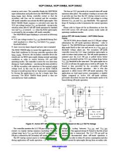
this device can be seen in Figure 43.
nd
1. The 2 order pole is present in small signal
gain−phase characteristics ≥ the lower cross over
frequency and worse transient response is imposed
by the system when voltage mode control is used.
There is no direct link to the actual primary current
– i.e. no line feed forward mechanism which
results in poor line transient response.
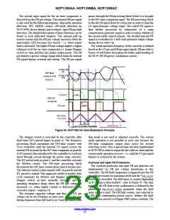
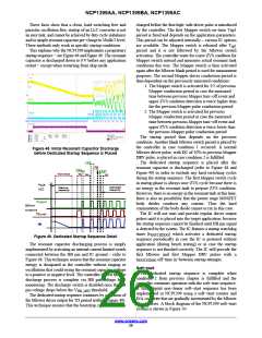
Figure 43. Internal Connection of the NCP1399 Current Mode Control Scheme
The basic principle of current mode control scheme
implementation lies in the use of an ON−time comparator
that defines upper switch on−time by comparing voltage
ramp, derived from the current sense input voltage, to the
divided feedback pin voltage. The upper switch on−time is
then re−used for low side switch conduction period. The
switching frequency is thus defined by the actual primary
current and output load conditions. Digital processing with
10 ns minimum on−time resolution is implemented to
ensure high noise immunity. The ON−time comparator
is divided down by capacitive divider (Ccs1, Ccs2, Rcs1,
Rcs2) before it is provided to the CS input. The capacitive
divider division ratio, which is fully externally adjustable,
defines the maximum primary current level that is reached
in case of maximum feedback voltage – i.e. the capacitive
divider division ration defines the maximum output power
of the converter for given bulk voltage. The CS is a bipolar
input pin which an input voltage swing is restricted to 5 V.
A fixed voltage offset is internally added to the CS pin signal
in order to assure enough voltage margin for operation the
feedback optocoupler − the FB optocoupler saturation voltage
is ~ 0.15 V (depending on type). However, the CS pin useful
signal for frequency modulation swings from 0 V, so current
mode regulation would not work under light load conditions
if no offset would be added to the CS pin before it is stabilized
to the level of the on−time comparator input. The CS pin
signal is also used for secondary side short circuit detection
– please refer to chapter dedicated to short circuit protection.
output is blanked by the leading edge blanking (t
) after
LEB
the Mupper switch is turned−on. The ON−time comparator
LEB period helps to avoid false triggering of the on−time
modulation due to noise generated by the HB pin voltage
transition.
The voltage signal for current sense input is prepared
externally via natural primary current integration by the
resonant tank capacitor Cs. The resonant capacitor voltage
www.onsemi.com
22

 ONSEMI [ ONSEMI ]