NCP1399AA, NCP1399BA, NCP1399AC
The latched OVP or OTP versions of NCP1399 enters
latched protection mode when V voltage cycles between
• Active OFF off−mode control − available on the
CC
NCP1399Ay device family
V
CC_ON
and V
thresholds and no pulses are provided
CC_OFF
These two off−mode operation control techniques differ in
the way the off−mode operation is started on the primary
side controller. Both of these methods are described
separately hereinafter.
by drivers. The controller VCC pin voltage has to be cycled
down below V threshold in order to restart
CC_RESET
operation. This would happen when the power supply is
unplugged from the mains.
Active ON Off−mode Control – NCP1399B Device
Family
SKIP/REM Input and Off−mode Control
The NCP1399 implements an ultra−low power
consumption mode of operation called off−mode. The
application output voltage is cycled between the nominal
and lower levels that are defined by the secondary side
off−mode controller (like NCP435x secondary off−mode
controller). The output voltage is thus not regulated to
nominal level but is always kept at a high enough voltage
level to provide bias for the necessary circuits in the target
application – for example this could be the case of
microcontroller with very low consumption that handles
VCC management in a notebook or TV. The no−load input
power consumption could be significantly reduced when
using described technique. The NCP1399 implements two
different off−mode control system approaches:
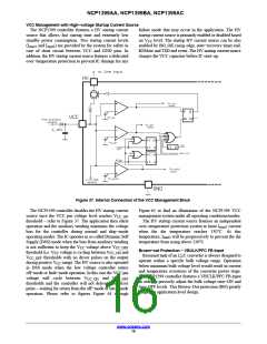
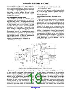
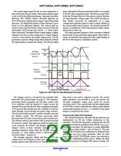
The NCP1399B device family uses a SKIP/REM pin only
for off−mode operation control– i.e. the pin is internally
connected to the Active ON off−mode control block and the
skip mode threshold level is not adjustable externally. The
skip mode comparator threshold can be adjusted only
internally (by IC option) in this package option. The
SKIP/REM pin when used for off−mode control allows the
user to activate the ultra−low consumption mode during
which the IC consumption is reduced to only very low HV
pin leakage current (I ) and very low VCC pin
HV_OFF−MODE
consumption (I
). The off*mode is activated
CC_OFF−MODE
when SKIP/REM pin voltage exceeds V
threshold.
REM_OFF
Normal operating mode is resumed when SKIP/REM pin
voltage drops below V threshold – refer to
REM_ON
• Active ON off−mode control − available on the
Figure 40 for an illustration.
NCP1399By device family
Figure 40. SKIP/REM Input Internal Connection – Active ON Version
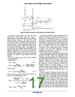
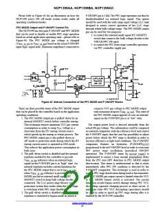
The off−mode operation is activated by the secondary side
off−mode controller. The auxiliary bias for primary side
off−mode control is provided by a circuit composed from
switching between ON−mode and OFF−mode states when
off−mode control is implemented. The OFF mode period
last significantly longer time (tens of seconds or more)
compared to the secondary capacitor refilling period (few
tens of milliseconds) – this explains why the no−load input
power consumption can be drastically reduced. The
auxiliary off−mode supply capacitor C1 can stay charged
while the secondary bias is lost – this can happen during
overload or other fault mode conditions. A REM TIMER is
thus implemented in the system to allow fast application
components D , C , R , R and C . The SKIP/REM pin is
2
1
1
2
2
pulled up by this auxiliary supply circuit once the REM
optocoupler (REM OK) is released. The application then
operates in off−mode until the secondary side off−mode
controller activates the REM optocoupler or until the
auxiliary bias on C is lost. Normal operation mode is then
1
recovered via power stage startup. The application is thus
www.onsemi.com
19

 ONSEMI [ ONSEMI ]