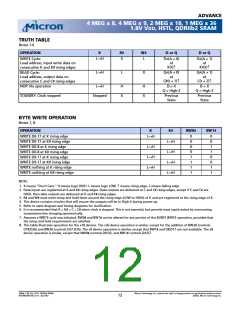
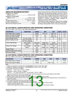
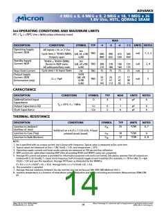
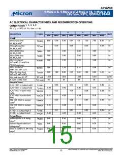
ADVANCE
4 MEG x 8, 4 MEG x 9, 2 MEG x 18, 1 MEG x 36
1.8V VDD, HSTL, QDRIIb2 SRAM
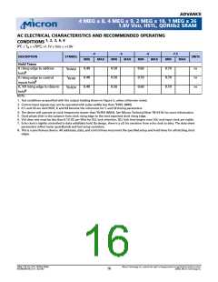
AC ELECTRICAL CHARACTERISTICS AND RECOMMENDED OPERATING
CONDITIONS 1, 2, 3, 6, 8
0ºC
?
TA
?
+70ºC; +1.7V ?ꢁVDD ? +1.9V
-4
-5
-6
-7.5
DESCRIPTION
SYMBOL
UNITS
MIN
0.40
0.40
0.40
MAX
MIN
0.50
0.50
0.50
MAX
MIN
0.60
0.70
0.60
MAX
MIN
0.70
0.70
0.70
MAX
Hold Times
K rising edge to address
hold8
K rising edge to control
inputs hold8
K, K# rising edge to data-in
tKHAX
tKHIX
ns
ns
ns
tKHDX
hold8
NOTE:
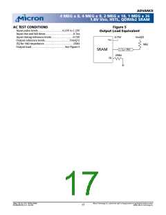
1. Test conditions as specified with the output loading shown in Figure 5, unless otherwise noted.
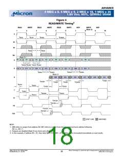
t
2. Control input signals may not be operated with pulse widths less than KHKL (MIN).
3. If C and C# are tied HIGH, K and K# become the references for C and C# timing parameters.
t
4. The device will operate at clock frequencies slower than KHKH (MAX). See Micron Technical Note TN-54-02 for more information.
5. Clock phase jitter is the variance from clock rising edge to the next expected clock rising edge.
6. VDD slew rate must be less than 0.1V DC per 50ns for DLL lock retention. DLL lock time begins once VDD and input clock are stable.
7. Echo clock is tightly controlled to data valid/data hold. By design, there is a 0.1ns variation from echo clock to data. The data sheet
parameters reflect tester guardbands and test setup variations.
8. This is a syncrhonous device. All addresses, data, and control lines must meet the specified setup and hold times for all latching clock
edges.
36Mb: 1.8V VDD, HSTL, QDRIIb2 SRAM
MT54W2MH18B_A.fm - Rev 9/02
Micron Technology, Inc., reserves the right to change products or specifications without notice.
©2002, Micron Technology Inc.
16

 MICRON [ MICRON TECHNOLOGY ]