ADVANCE
4 MEG x 8, 4 MEG x 9, 2 MEG x 18, 1 MEG x 36
1.8V VDD, HSTL, QDRIIb2 SRAM
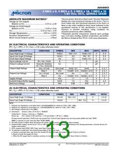
*Stresses greater than those listed under Absolute Maximum
ABSOLUTE MAXIMUM RATINGS*
Ratings may cause permanent damage to the device. This is a
stress rating only, and functional operation of the device at
these or any other conditions above those indicated in the
operational sections of this specification is not implied.
Exposure to absolute maximum rating conditions for
extended periods may affect reliability.
**Maximum junction temperature depends upon package
type, cycle time, loading, ambient temperature, and airflow.
See Micron Technical Note TN-05-14 for more information.
Voltage on VDD Supply
Relative to VSS ........................................ 0.5V to +2.8V
Voltage on VDDQ Supply
Relative to VSS ....................................... -0.5V to +VDD
VIN ..................................................... -0.5V to VDD + 0.5V
Storage Temperature..............................-55ºC to +125ºC
Junction Temperature**....................................... +125ºC
Short Circuit Output Current .............................. 70mA
DC ELECTRICAL CHARACTERISTICS AND OPERATING CONDITIONS
0ºC
?
TA
?
+70ºC; +1.7V ? VDD ? +1.9V unless otherwise noted
DESCRIPTION
CONDITIONS
SYMBOL
MIN
MAX
UNITS NOTES
VIH(DC)
VIL(DC)
VIN
VREF + 0.1
VDDQ + 0.3
V
V
3, 4
3, 4
3, 4
Input High (Logic 1) Voltage
Input Low (Logic 0) Voltage
Clock Input Signal Voltage
Input Leakage Current
-0.3
-0.3
-5
VREF - 0.1
VDDQ + 0.3
V
0V ? VIN ? VDDQ
ILI
5
5
µA
µA
Output(s) disabled,
ILO
-5
Output Leakage Current
0V ? VIN ? VDDQ (Q)
|IOH| ? 0.1mA
Note 1
VOH (LOW)
VOH
VDDQ - 0.2
VDDQ/2 - 0.12
VSS
VDDQ
VDDQ/2 + 0.12
0.2
V
V
V
V
V
V
V
3, 5, 7
3, 5, 7
3, 5, 7
3, 5, 7
3
Output High Voltage
Output Low Voltage
IOL ? 0.1mA
Note 2
VOL (LOW)
VOL
VDDQ/2 - 0.12
1.7
VDDQ/2 + 0.12
1.9
Supply Voltage
VDD
Isolated Output Buffer Supply
Reference Voltage
VDDQ
VREF
1.4
VDD
3, 6
0.68
0.95
3
AC ELECTRICAL CHARACTERISTICS AND OPERATING CONDITIONS
0ºC
?
TA
?
+70ºC; +1.7V ? VDD ? +1.9V unless otherwise noted
DESCRIPTION
CONDITIONS
SYMBOL
VIH AC)
MIN
VREF + 0.2
–
MAX
–
UNITS
NOTES
3, 4, 8
3, 4, 8
V
V
Input High (Logic 1) Voltage
Input Low (Logic 0) Voltage
NOTE:
VIL(AC)
VREF - 0.2
1. Outputs are impedance-controlled. |IOH| = (VDDQ/2)/(RQ/5) for values of 175ꢀ ? RQ ? 350ꢀ.
2. Outputs are impedance-controlled. IOL = (VDDQ/2)/(RQ/5) for values of 175ꢀ ? RQ ? 350ꢀ.
3. All voltages referenced to VSS (GND).
t
4. Overshoot:
VIH(AC) ? VDD + 0.7V for t ? KHKH/2
t
Undershoot: VIL(AC)ꢁO -0.5V for t ? KHKH/2
Power-up:
VIH ? VDDQ + 0.3V and VDD ? 1.7V and VDDQ ? 1.4V for t ? 200ms
t
During normal operation, VDDQ must not exceed VDD. Control input signals may not have pulse widths less than KHKL
t
(MIN) or operate at cycle rates less than KHKH (MIN).
5. AC load current is higher than the shown DC values. AC I/O curves are available upon request.
6. Output buffer supply can be set to 1.5V or 1.8V nominal 0.1 with appropriate derating of AC timing parameters. Consult factory for
further information.
7. HSTL outputs meet JEDEC HSTL Class I and Class II standards.
8. To maintain a valid level, the transitioning edge of the input must:
a. Sustain a constant slew rate from the current AC level through the target AC level, VIL(AC) or VIH(AC).
b. Reach at least the target AC level.
c. After the AC target level is reached, continue to maintain at least the target DC level, VIL(DC) or VIH(DC).
36Mb: 1.8V VDD, HSTL, QDRIIb2 SRAM
MT54W2MH18B_A.fm - Rev 9/02
Micron Technology, Inc., reserves the right to change products or specifications without notice.
©2002, Micron Technology Inc.
13

 MICRON [ MICRON TECHNOLOGY ]