ADVANCE
4 MEG x 8, 4 MEG x 9, 2 MEG x 18, 1 MEG x 36
1.8V VDD, HSTL, QDRIIb2 SRAM
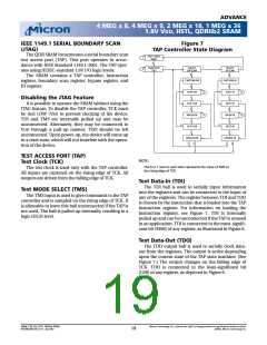
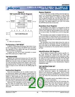
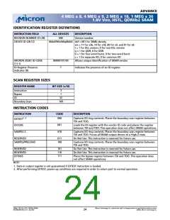
Figure 8
TAP Controller Block Diagram
Bypass Register
To save time when serially shifting data through reg-
isters, it is sometimes advantageous to skip certain
chips. The bypass register is a single-bit register that
can be placed between the TDI and TDO balls. This
allows data to be shifted through the SRAM with mini-
mal delay. The bypass register is set LOW (VSS) when
the BYPASS instruction is executed.
0
Bypass Register
2
1 0
Selection
Circuitry
Selection
Circuitry
Instruction Register
31 30 29
Identification Register
TDI
TDO
.
.
. 2 1 0
x
.
.
.
.
. 2 1 0
Boundary Scan Register
The boundary scan register is connected to all the
input and bidirectional balls on the SRAM. Several no
connect (NC) balls are also included in the scan regis-
ter to reserve balls. The SRAM has a 109-bit-long regis-
ter.
Boundary Scan Register
TCK
TMS
TAP CONTROLLER
The boundary scan register is loaded with the con-
tents of the RAM I/O ring when the TAP controller is in
the Capture-DR state and is then placed between the
TDI and TDO balls when the controller is moved to the
Shift-DR state.
NOTE:
X = 108 for all configurations.
The Boundary Scan Order tables show the order in
which the bits are connected. Each bit corresponds to
one of the balls on the SRAM package. The MSB of the
register is connected to TDI, and the LSB is connected
to TDO.
Performing a TAP RESET
A RESET is performed by forcing TMS HIGH (VDD)
for five rising edges of TCK. This RESET does not affect
the operation of the SRAM and may be performed
while the SRAM is operating.
Identification (ID) Register
At power-up, the TAP is reset internally to ensure
that TDO comes up in a High-Z state.
The ID register is loaded with a vendor-specific, 32-
bit code during the Capture-DR state when the
IDCODE command is loaded in the instruction regis-
ter. The IDCODE is hardwired into the SRAM and can
be shifted out when the TAP controller is in the Shift-
DR state. The ID register has a vendor code and other
information described in the Identification Register
Definitions table.
TAP REGISTERS
Registers are connected between the TDI and TDO
balls and allow data to be scanned into and out of the
SRAM test circuitry. Only one register can be selected
at a time through the instruction register. Data is seri-
ally loaded into the TDI ball on the rising edge of TCK.
Data is output on the TDO ball on the falling edge of
TCK.
TAP INSTRUCTION SET
Overview
Eight different instructions are possible with the
three-bit instruction register. All combinations are
listed in the Instruction Codes table. Three of these
instructions are listed as RESERVED and should not be
used. The other five instructions are described below
in detail.
The TAP controller used in this SRAM is fully com-
pliant to the 1149.1 convention.
Instructions are loaded into the TAP controller dur-
ing the Shift-IR state when the instruction register is
placed between TDI and TDO. During this state,
instructions are shifted through the instruction regis-
Instruction Register
Three-bit instructions can be serially loaded into
the instruction register. This register is loaded when it
is placed between the TDI and TDO balls as shown in
Figure 8. Upon power-up, the instruction register is
loaded with the IDCODE instruction. It is also loaded
with the IDCODE instruction if the controller is placed
in a reset state, as described in the previous section.
When the TAP controller is in the Capture-IR state,
the two LSBs are loaded with a binary “01” pattern to
allow for fault isolation of the board-level serial test
data path.
36Mb: 1.8V VDD, HSTL, QDRIIb2 SRAM
MT54W2MH18B_A.fm - Rev 9/02
Micron Technology, Inc., reserves the right to change products or specifications without notice.
©2002, Micron Technology Inc.
20

 MICRON [ MICRON TECHNOLOGY ]