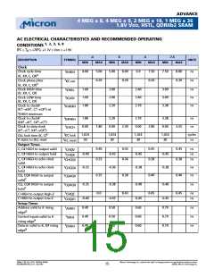
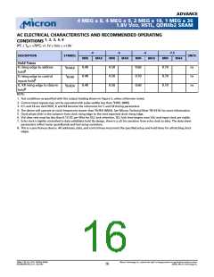
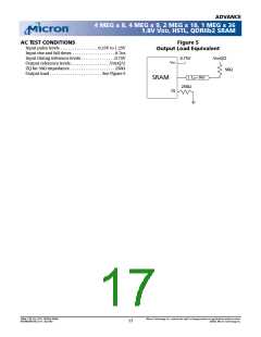
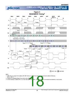
ADVANCE
4 MEG x 8, 4 MEG x 9, 2 MEG x 18, 1 MEG x 36
1.8V VDD, HSTL, QDRIIb2 SRAM
IEEE 1149.1 SERIAL BOUNDARY SCAN
(JTAG)
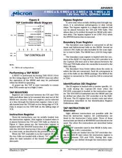
Figure 7
TAP Controller State Diagram
The QDR SRAM incorporates a serial boundary scan
TEST-LOGIC
RESET
1
0
test access port (TAP). This port operates in accor-
dance with IEEE Standard 1149.1-2001. The TAP oper-
ates using JEDEC-standard 1.8V I/O logic levels.
The SRAM contains a TAP controller, instruction
register, boundary scan register, bypass register, and
ID register.
0
1
1
1
RUN-TEST/
IDLE
SELECT
SELECT
IR-SCAN
DR-SCAN
0
0
1
1
CAPTURE-DR
CAPTURE-IR
0
0
SHIFT-DR
0
SHIFT-IR
0
1
1
Disabling the JTAG Feature
1
1
EXIT1-DR
EXIT1-IR
It is possible to operate the SRAM without using the
JTAG feature. To disable the TAP controller, TCK must
be tied LOW (VSS) to prevent clocking of the device.
TDI and TMS are internally pulled up and may be
unconnected. Alternately, they may be connected to
VDD through a pull-up resistor. TDO should be left
unconnected. Upon power-up, the device will come up
in a reset state, which will not interfere with the opera-
tion of the device.
0
0
PAUSE-DR
1
0
PAUSE-IR
1
0
0
0
EXIT2-DR
1
EXIT2-IR
1
UPDATE-DR
UPDATE-IR
1
0
1
0
TEST ACCESS PORT (TAP)
Test Clock (TCK)
NOTE:
The 0 or 1 next to each state represents the value of TMS at
the rising edge of TCK.
The test clock is used only with the TAP controller.
All inputs are captured on the rising edge of TCK. All
outputs are driven from the falling edge of TCK.
Test Data-In (TDI)
The TDI ball is used to serially input information
into the registers and can be connected to the input of
any of the registers. The register between TDI and TDO
is chosen by the instruction that is loaded into the TAP
instruction register. For information on loading the
instruction register, see Figure 7. TDI is internally
pulled up and can be unconnected if the TAP is unused
in an application. TDI is connected to the most-signifi-
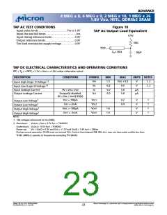
cant bit (MSB) of any register, as illustrated in Figure 8.
Test MODE SELECT (TMS)
The TMS input is used to give commands to the TAP
controller and is sampled on the rising edge of TCK. It
is allowable to leave this ball unconnected if the TAP is
not used. The ball is pulled up internally, resulting in a
logic HIGH level.
Test Data-Out (TDO)
The TDO output ball is used to serially clock data-
out from the registers. The output is active depending
upon the current state of the TAP state machine. (See
Figure 7.) The output changes on the falling edge of
TCK. TDO is connected to the least-significant bit
(LSB) of any register, as depicted in Figure 8.
36Mb: 1.8V VDD, HSTL, QDRIIb2 SRAM
MT54W2MH18B_A.fm - Rev 9/02
Micron Technology, Inc., reserves the right to change products or specifications without notice.
©2002, Micron Technology Inc.
19

 MICRON [ MICRON TECHNOLOGY ]