ADVANCE
4 MEG x 8, 4 MEG x 9, 2 MEG x 18, 1 MEG x 36
1.8V VDD, HSTL, QDRIIb2 SRAM
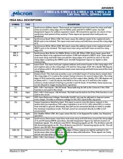
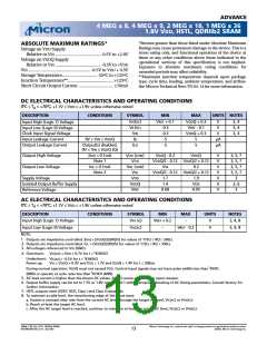
TRUTH TABLE
Notes 1-6
OPERATION
K
R#
W#
D or Q
D or Q
LJH
X
L
DA(A + 0)
at
K(t)I
DA(A + 1)
at
K#(t)I
WRITE Cycle:
Load address, input write data on
consecutive K and K# rising edges
LJH
L
X
QA(A + 0)
at
C#(t + 1)I
QA(A + 1)
at
C(t + 2)I
READ Cycle:
Load address, output data on
consecutive C and C# rising edges
NOP: No operation
LJH
H
X
H
X
D = X
Q = High-Z
D = X
Q = High-Z
STANDBY: Clock stopped
Stopped
Previous
State
Previous
State
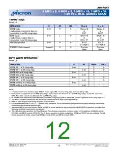
BYTE WRITE OPERATION
Notes 7, 8
OPERATION
K
K#
BW0#
BW1#
LJH
0
0
0
0
1
1
1
1
0
0
1
1
0
0
1
1
WRITE D0-17 at K rising edge
WRITE D0-17 at K# rising edge
WRITE D0-8 at K rising edge
WRITE D0-8 at K# rising edge
WRITE D9-17 at K rising edge
WRITE D9-17 at K# rising edge
WRITE nothing at K rising edge
WRITE nothing at K# rising edge
LJH
LJH
LJH
LJH
LJH
LJH
LJH
NOTE:
1. X means “Don’t Care.” H means logic HIGH. L means logic LOW. I means rising edge; K means falling edge.
2. Data inputs are registered at K and K# rising edges. Data outputs are delivered at C and C# rising edges, except if C and C# are
HIGH, then data outputs are delivered at K and K# rising edges.
3. R# and W# must meet setup and hold times around the rising edge (LOW to HIGH) of K and are registered at the rising edge of K.
4. This device contains circuitry that will ensure the outputs will be in High-Z during power-up.
5. Refer to state diagram and timing diagrams for clarification.
6. It is recommended that K = K# = C = C# when clock is stopped. This is not essential, but permits most rapid restart by overcoming
transmission line charging symmetrically.
7. Assumes a WRITE cycle was initiated. BW0# and BW1# can be altered for any portion of the BURST WRITE operation, provided that
the setup and hold requirements are satisfied.
8. This table illustrates operation for the x18 devices. The x36 device operation is similar, except for the addition of BW2# (controls
D18:D26) and BW3# (controls D27:D35). The x9 device operation is similar, except that BW1# and D8:D17 are not available. The x8
device operation is similar, except that NW0# controls D0:D3, and NW1# controls D4:D7.
36Mb: 1.8V VDD, HSTL, QDRIIb2 SRAM
MT54W2MH18B_A.fm - Rev 9/02
Micron Technology, Inc., reserves the right to change products or specifications without notice.
©2002, Micron Technology Inc.
12

 MICRON [ MICRON TECHNOLOGY ]