ADVANCE
4 MEG x 8, 4 MEG x 9, 2 MEG x 18, 1 MEG x 36
1.8V VDD, HSTL, QDRIIb2 SRAM
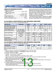
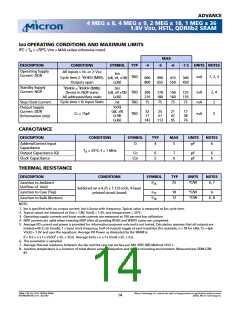
IDD OPERATING CONDITIONS AND MAXIMUM LIMITS
0ºC
?
TA
?
+70ºC; VDD = MAX unless otherwise noted
MAX
DESCRIPTION
CONDITIONS
SYMBOL
TYP
-4
-5
-6
-7.5 UNITS NOTES
Operating Supply
Current: DDR
All inputs ? VIL or O VIH;
IDD
(x8, x9, x18)
(x36)
t
TBD
mA
1, 2, 3
Cycle time Oꢀ KHKH (MIN);
600
800
490
655
415
550
340
450
Outputs open
tKHKH = tKHKH (MIN);
Device in NOP state;
All addresses/data static
ISB1
(x8, x9 x18)
(x36)
Standby Supply
Current: NOP
TBD
TBD
mA
mA
2, 4
2
200
210
170
180
150
160
125
135
Cycle time = 0; Input Static
Stop Clock Current
ISB
75
75
75
75
IDDQ
(x8, x9)
(x18)
Output Supply
Current: DDR
(Information only)
32
71
142
25
57
113
21
47
95
17
38
76
CL = 15pF
TBD
mA
5
(x36)
CAPACITANCE
DESCRIPTION
CONDITIONS
SYMBOL
TYP
MAX
UNITS
NOTES
CI
4
5
pF
6
Address/Control Input
Capacitance
TA = 25ºC; f = 1 MHz
Output Capacitance (Q)
Clock Capacitance
CO
6
5
7
6
pF
pF
6
6
CCK
THERMAL RESISTANCE
DESCRIPTION
CONDITIONS
SYMBOL
TYP
UNITS
NOTES
ꢀJA
25
ºC/W
6, 7
Junction to Ambient
(Airflow of 1m/s)
Soldered on a 4.25 x 1.125 inch, 4-layer
printed circuit board
Junction to Case (Top)
Junction to Balls (Bottom)
NOTE:
ꢀ
JC
10
12
ºC/W
ºC/W
6
ꢀ
JB
6, 8
1. IDD is specified with no output current. IDD is linear with frequency. Typical value is measured at 6ns cycle time.
2. Typical values are measured at VDD = 1.8V, VDDQ = 1.5V, and temperature = 25°C.
3. Operating supply currents and burst mode currents are measured at 100 percent bus utilization.
4. NOP currents are valid when entering NOP after all pending READ and WRITE cycles are completed.
5. Average I/O current and power is provided for information purposes only and is not tested. Calculation assumes that all outputs are
loaded with CL (in farads), f = input clock frequency, half of outputs toggle at each transition (for example, n = 18 for x36), CO = 6pF,
VDDQ = 1.5V and uses the equations: Average I/O Power as dissipated by the SRAM is:
2
P = 0.5 × n x f x VDDQ x (CL + 2CO). Average IDDQ = n x f x VDDQ x (CL + CO).
6. This parameter is sampled.
7. Average thermal resistance between the die and the case top surface per MIL SPEC 883 Method 1012.1.
8. Junction temperature is a function of total device power dissipation and device mounting environment. Measured per SEMI G38-
87.
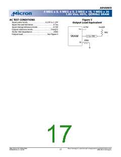
36Mb: 1.8V VDD, HSTL, QDRIIb2 SRAM
MT54W2MH18B_A.fm - Rev 9/02
Micron Technology, Inc., reserves the right to change products or specifications without notice.
©2002, Micron Technology Inc.
14

 MICRON [ MICRON TECHNOLOGY ]