4 MEG x 4
FPM DRAM
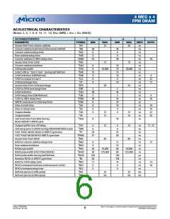
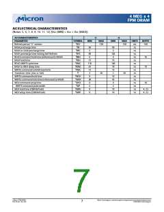
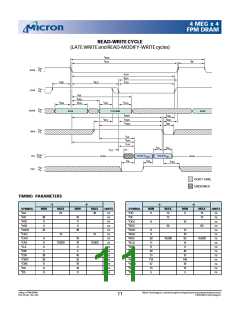
AC ELECTRICAL CHARACTERISTICS
(Notes: 5, 6, 7, 8, 9, 10, 11, 12) [Vcc (MIN) £ Vcc £ Vcc (MAX)]
ACCHARACTERISTICS
-5
-6
PARAMETER
SYMBOL
MIN
MAX
MIN
MAX
UNITS
ms
ns
NOTES
t
Refresh period “S” version
RAS# precharge time
REF
128
128
140
t
RP
30
5
40
5
t
RAS# to CAS# precharge time
RAS# precharge time exiting Self Refresh
READcommand hold time (referenced to RAS#)
RAS# hold time
RPC
ns
t
RPS
90
0
105
0
ns
t
RRH
ns
16
19
t
RSH
13
116
67
13
2
15
140
79
15
2
ns
t
READ-WRITE cycle time
RWC
ns
t
RAS# to WE# delay time
RWD
ns
t
WRITE command to RAS# lead time
Transition time (rise or fall)
WRITEcommand hold time
WRITE command hold time (referenced to RAS#)
WE# command setup time
RWL
ns
t
T
50
50
ns
t
WCH
8
10
45
0
ns
t
WCR
38
0
ns
t
WCS
ns
18
t
WRITEcommand pulse width
WE# hold time (CBR Refresh)
WE# setup time (CBR Refresh)
WP
5
5
ns
t
WRH
8
10
10
ns
4, 23
4, 23
t
WRP
8
ns
4 Meg x 4 FPM DRAM
D49_5V.p65 – Rev. 5/00
Micron Technology, Inc., reservesthe right to change productsor specificationswithout notice.
©2000, Micron Technology, Inc.
7

 MICRON [ MICRON TECHNOLOGY ]