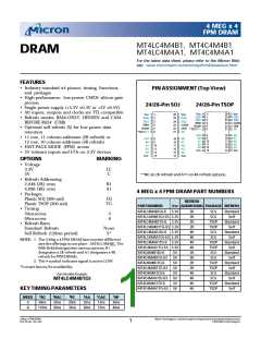
4 MEG x 4
FPM DRAM
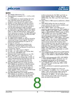
*Stresses greater th an th ose listed un der “Absolute Maxi-
m um Ratin gs” m ay cause perm an en t dam age to th e
device. Th is is a stress ratin g on ly, an d fun ction al opera-
tion of th e device at th ese or an y oth er con dition s above
th ose in dicated in th e operation al section s of th is speci-
fication is n ot im plied. Exposure to absolute m axim um
ratin g con dition s for exten ded periods m ay affect
reliability.
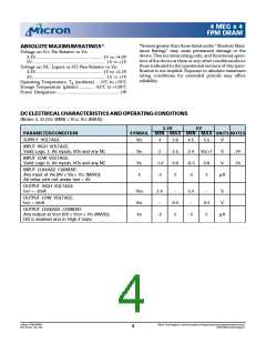
ABSOLUTEMAXIMUM RATINGS*
Voltage on VCC Pin Relative to VSS
3.3V............................................. ......... -1V to +4.6V
5V................................................ ............ -1V TO +7V
Voltage on NC, In puts or I/O Pin s Relative to VSS
3.3V............................................. ......... -1V to +5.5V
5V................................................ ............ -1V TO +7V
Operatin g Tem perature, TA (am bien t) .... 0°C to +70°C
Storage Tem perature (plastic) ............ -55°C to +150°C
Power Dissipation ................................................... 1W
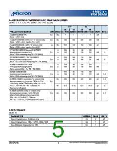
DC ELECTRICAL CHARACTERISTICS AND OPERATING CONDITIONS
(Notes: 5, 6) (VCC (MIN) £ VCC£ VCC (MAX))
3.3V
5 V
PARAMETER/CONDITION
SYMBOL M IN M AX M IN M AX UNITS NOTES
SUPPLY VOLTAGE
VCC
VIH
VIL
II
3
3.6
5.5
0.8
2
4.5
2.4
-0.5
-2
5.5
Vcc+1
0.8
V
INPUT HIGH VOLTAGE:
Valid Logic 1; All inputs, I/Os and any NC
2
V
24
24
INPUT LOW VOLTAGE:
Valid Logic 0; All inputs, I/Os and any NC
-1.0
-2
V
INPUT LEAKAGE CURRENT:
Any input at VIN [0V £ VIN £ VCC (MAX)];
All other pins not under test = 0V
2
µA
OUTPUT HIGH VOLTAGE:
IOUT = -2mA
VOH
VOL
IOZ
2.4
–
–
0.4
5
2.4
–
–
0.4
5
V
V
OUTPUT LOW VOLTAGE:
IOUT = 2mA
OUTPUT LEAKAGE CURRENT:
Any output at VOUT [0V £ VOUT £ VCC (MAX)];
DQ is disabled and in High-Z state
-5
-5
µA
4 Meg x 4 FPM DRAM
D49_5V.p65 – Rev. 5/00
Micron Technology, Inc., reservesthe right to change productsor specificationswithout notice.
©2000, Micron Technology, Inc.
4

 MICRON [ MICRON TECHNOLOGY ]