4 MEG x 4
FPM DRAM
NOTES
1. All voltages referen ced to VSS.
t
t
trolled exclusively by AA (tRAC an d CAC n o
2. Th is param eter is sam pled. VCC = +3.3V or 5.0V;
f = 1 MHz.
t
lon ger applied). With or with out th e RAD
(MAX) lim it, AA, RAC, an d CAC m ust always
be m et.
t
t
t
3. ICC is depen den t on output loadin g an d cycle
rates. Specified values are obtain ed with
m in im um cycle tim e an d th e outputs open .
4. En ables on -ch ip refresh an d address coun ters.
5. Th e m in im um specification s are used on ly to
in dicate cycle tim e at wh ich proper operation
over th e full tem perature ran ge is en sured.
6. An in itial pause of 100µs is required after power-
up, followed by eigh t RAS# refresh cycles (RAS#-
ONLY or CBR with WE# HIGH), before proper
device operation is en sured. Th e eigh t RAS# cycle
t
t
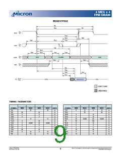
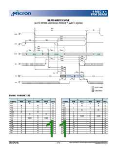
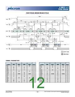
16. Eith er RCH or RRH m ust be satisfied for a READ
cycle.
17. OFF (MAX) defin es th e tim e at wh ich th e
output ach ieves th e open circuit con dition an d
is n ot referen ced to VOH or VOL.
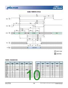
18. WCS, RWD, AWD, an d CWD are n ot
t
t
t
t
t
t
restrictive operatin g param eters. WCS applies to
t
t
t
EARLY WRITE cycles. RWD, AWD, an d CWD
t
apply to READ-MODIFY-WRITE cycles. If WCS
tWCS (MIN), th e cycle is an EARLY WRITE
t
wake-ups sh ould be repeated an y tim e th e REF
refresh requirem en t is exceeded.
7. AC ch aracteristics assum e T = 5n s.
cycle an d th e data output will rem ain an open
t
circuit th rough out th e en tire cycle. If RWD ³
t
tRWD (MIN), AWD ³ tAWD (MIN), an d tCWD
t
8. VIH (MIN) an d VIL (MAX) are referen ce levels for
m easurin g tim in g of in put sign als. Tran sition
tim es are m easured between VIH an d VIL (or
between VIL an d VIH).
9. In addition to m eetin g th e tran sition rate
specification , all in put sign als m ust tran sit
between VIH an d VIL (or between VIL an d VIH) in
a m on oton ic m an n er.
10. If CAS# = VIH, data output is High -Z.
11. If CAS# = VIL, data output m ay con tain data
from th e last valid READ cycle.
12. Measured with a load equivalen t to two TTL
gates, 100pF an d VOL = 0.8V an d VOH = 2V.
13. If CAS# is LOW at th e fallin g edge of RAS#, Q
will be m ain tain ed from th e previous cycle. To
in itiate a n ew cycle an d clear th e data-out
³ tCWD (MIN), th e cycle is a READ-MODIFY-
WRITE an d th e data output will con tain data
read from th e selected cell. If n eith er of th e
above con dition s is m et, th e state of data-out is
in determ in ate. OE# h eld HIGH an d WE# taken
LOW after CAS# goes LOW result in a LATE
t
t
WRITE (OE#-con trolled) cycle. WCS, RWD,
tCWD, an d AWD are n ot applicable in a LATE
t
WRITE cycle.
19. Th ese param eters are referen ced to CAS# leadin g
edge in EARLY WRITE cycles an d WE# leadin g
edge in LATE WRITE or READ-MODIFY-WRITE
cycles.
20. If OE# is tied perm an en tly LOW, LATE WRITE,
or READ-MODIFY-WRITE operation s are n ot
perm issible an d sh ould n ot be attem pted.
21. A HIDDEN REFRESH m ay also be perform ed
after a WRITE cycle. In th is case, WE# = LOW
an d OE# = HIGH.
t
buffer, CAS# m ust be pulsed HIGH for CP.
t
14. Th e RCD (MAX) lim it is n o lon ger specified.
tRCD (MAX) was specified as a referen ce poin t
t
on ly. If RCD was greater th an th e specified
22. Th e 3n s m in im um is a param eter guaran teed by
design .
tRCD (MAX) lim it, th en access tim e was con -
trolled exclusively by CAC (tRAC [MIN] n o
t
23. Colum n address ch an ged on ce each cycle.
24. VIH oversh oot: VIH (MAX) = VCC + 2V for a pulse
width £ 10n s, an d th e pulse width can n ot be
greater th an on e th ird of th e cycle rate. VIL
un dersh oot: VIL (MIN) = -2V for a pulse width £
10n s, an d th e pu lse width can n ot be greater
th an on e th ird of th e cycle rate.
t
lon ger applied). With or with out th e RCD lim it,
tAA an d CAC m ust always be m et.
t
t
15. Th e RAD (MAX) lim it is n o lon ger specified.
tRAD (MAX) was specified as a referen ce poin t
t
on ly. If RAD was greater th an th e specified
tRAD (MAX) lim it, th en access tim e was con -
4 Meg x 4 FPM DRAM
D49_5V.p65 – Rev. 5/00
Micron Technology, Inc., reservesthe right to change productsor specificationswithout notice.
©2000, Micron Technology, Inc.
8

 MICRON [ MICRON TECHNOLOGY ]