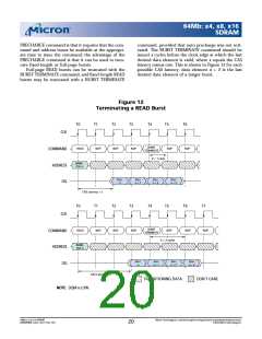
64Mb : x4, x8, x16
SDRAM
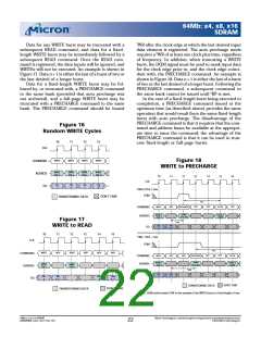
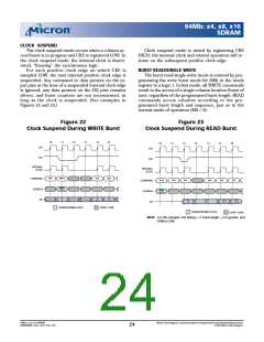
CLOCK SUSPEND
The clock suspend m ode occurs when a colum n ac-
cess/ burst is in progress and CKE is registered LOW. In
the clock suspend m ode, the internal clock is deacti-
vated, “freezing” the synchronous logic.
Clock suspend m ode is exited by registering CKE
HIGH; the internal clock and related operation will re-
sum e on the subsequent positive clock edge.
For each p ositive clock edge on wh ich CKE is
sam pled LOW, the next internal positive clock edge is
suspended. Any com m and or data present on the in-
put pins at the tim e of a suspended internal clock edge
is ignored; any data present on the DQ pins rem ains
driven; and burst counters are not increm ented, as
lon g as th e clock is su sp en ded. (See exam p les in
Figures 22 and 23.)
BURST READ/SINGLE WRITE
The burst read/ single write m ode is entered by pro-
gram m ing the write burst m ode bit (M9) in the m ode
register to a logic 1. In this m ode, all WRITE com m ands
result in the access of a single colum n location (burst of
one), regardless of the program m ed burst length. READ
com m an ds access colu m n s accordin g to th e p ro-
gram m ed burst length and sequence, just as in the
norm al m ode of operation (M9 = 0).
Fig u re 22
Fig u re 23
Clo ck Su sp e n d Du rin g WRITE Bu rst
Clo ck Su sp e n d Du rin g READ Bu rst
T0
T1
T2
T3
T4
T5
T0
T1
T2
T3
T4
T5
T6
CLK
CKE
CLK
CKE
INTERNAL
CLOCK
INTERNAL
CLOCK
NOP
WRITE
NOP
NOP
COMMAND
ADDRESS
READ
NOP
NOP
NOP
NOP
NOP
COMMAND
ADDRESS
DQ
BANK,
COL n
BANK,
COL n
DIN
DIN
DIN
n + 2
DIN
D
OUT
D
n
OUT
D
n
OUT
D
n
OUT
n
n
+ 1
n
+ 1
+ 2
+ 3
TRANSITIONING DATA
DON’T CARE
TRANSITIONING DATA
DON’T CARE
NOTE: For this example, CAS latency = 2, burst length = 4 or greater, and
DQM is LOW.
64Mb: x4, x8, x16 SDRAM
64MSDRAM_F.p65 – Rev. F; Pub. 1/03
Micron Technology, Inc., reservesthe right to change productsor specificationswithout notice.
©2003, Micron Technology, Inc.
24

 MICRON [ MICRON TECHNOLOGY ]