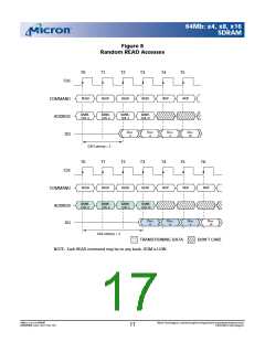
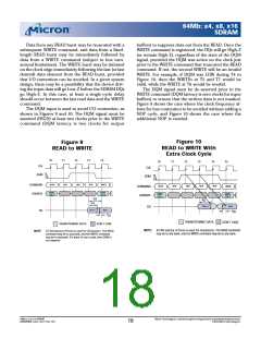
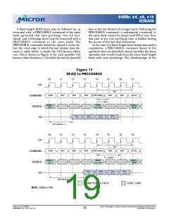
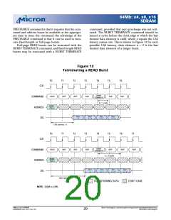
64Mb : x4, x8, x16
SDRAM
WRITEs
WRITE bursts are initiated with a WRITE com m and,
as shown in Figure 13.
An exam ple is shown in Figure 15. Data n + 1 is either
the last of a burst of two or the last desired of a longer
burst. The 64Mb SDRAM uses a pipelined architecture
and therefore does not require the 2n rule associated
with a prefetch architecture. A WRITE com m and can
be initiated on any clock cycle following a previous
WRITE com m and. Full-speed random write accesses
within a page can be perform ed to the sam e bank, as
shown in Figure 16, or each subsequent WRITE m ay be
perform ed to a different bank.
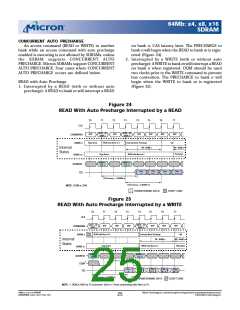
Th e startin g colu m n an d b an k ad d resses are
p rovid ed with th e WRITE com m an d , an d au to
precharge is either enabled or disabled for that access.
If auto precharge is enabled, the row being accessed is
precharged at the com pletion of the burst. For the ge-
neric WRITE com m ands used in the following illustra-
tions, auto precharge is disabled.
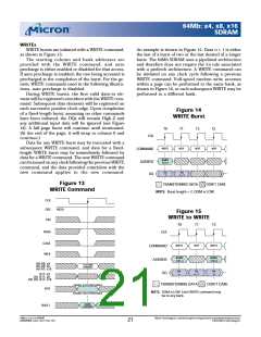
During WRITE bursts, the first valid data-in ele-
m ent will be registered coincident with the WRITE com -
m and. Subsequent data elem ents will be registered on
each successive positive clock edge. Upon com pletion
of a fixed-length burst, assum ing no other com m ands
have been initiated, the DQs will rem ain High-Z and
any additional input data will be ignored (see Figure
14). A full-page burst will continue until term inated.
(At the end of the page, it will wrap to colum n 0 and
con tin ue.)
Fig u re 14
WRITE Bu rst
T0
T1
T2
T3
CLK
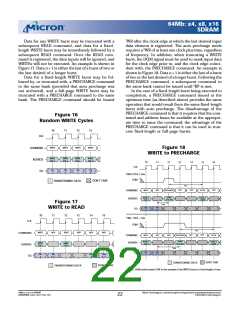
Data for any WRITE burst m ay be truncated with a
subsequent WRITE com m and, and data for a fixed-
length WRITE burst m ay be im m ediately followed by
data for a WRITE com m and. The new WRITE com m and
can be issued on any clock following the previous WRITE
com m and, and the data provided coincident with the
n ew com m an d ap p lies to th e n ew com m an d .
WRITE
NOP
NOP
NOP
COMMAND
ADDRESS
DQ
BANK,
COL n
DIN
DIN
n + 1
n
Fig u re 13
TRANSITIONING DATA
DON’T CARE
WRITE Co m m a n d
NOTE: Burst length = 2. DQM is LOW.
CLK
CKE
CS#
HIGH
Fig u re 15
WRITE t o WRITE
T0
T1
T2
RAS#
CLK
CAS#
WE#
WRITE
NOP
WRITE
COMMAND
ADDRESS
DQ
BANK,
COL n
BANK,
COL b
A0-A9: x4
A0-A8: x8
A0-A7: x16
COLUMN
ADDRESS
DIN
DIN
DIN
b
A11: x4
A9, A11: x8
A8, A9, A11: x16
n
n + 1
TRANSITIONING DATA
DON’T CARE
ENABLE AUTO PRECHARGE
DISABLE AUTO PRECHARGE
A10
NOTE: DQM is LOW. Each WRITE command may
be to any bank.
BANK
ADDRESS
BA0,1
64Mb: x4, x8, x16 SDRAM
64MSDRAM_F.p65 – Rev. F; Pub. 1/03
Micron Technology, Inc., reservesthe right to change productsor specificationswithout notice.
©2003, Micron Technology, Inc.
21

 MICRON [ MICRON TECHNOLOGY ]