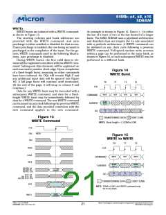
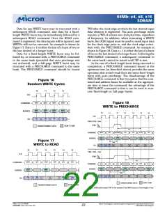
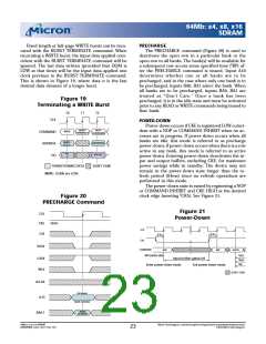
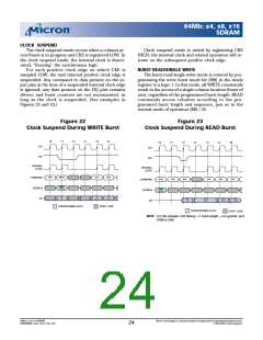
64Mb : x4, x8, x16
SDRAM
CONCURRENT AUTO PRECHARGE
An access com m and (READ or WRITE) to another
bank while an access com m and with auto precharge
enabled is executing is not allowed by SDRAMs, unless
th e SDRAM su p p orts CONCURRENT AUTO
PRECHARGE. Micron SDRAMs support CONCURRENT
AUTO PRECHARGE. Four cases where CONCURRENT
AUTO PRECHARGE occurs are defined below.
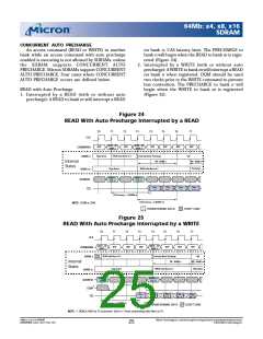
on bank n, CAS latency later. The PRECHARGE to
bank n will begin when the READ to bank m is regis-
tered (Figure 24).
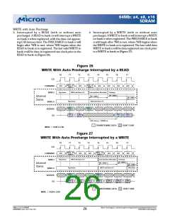
2. In terrup ted by a WRITE (with or with out auto
precharge): A WRITE to bank m will interrupt a READ
on bank n when registered. DQM should be used
two clocks prior to the WRITE com m and to prevent
bus contention. The PRECHARGE to bank n will
begin when the WRITE to ban k m is registered
(Figure 25).
READ with Auto Precharge
1. In terru p ted b y a READ (with or with ou t au to
precharge): A READ to bank m will interrupt a READ
Fig u re 24
READ Wit h Au t o Pre ch a rg e In t e rru p t e d b y a READ
T0
T1
T2
T3
T4
T5
T6
T7
CLK
READ - AP
BANK n
READ - AP
BANK m
NOP
NOP
NOP
NOP
NOP
NOP
COMMAND
Page Active
READ with Burst of 4
Interrupt Burst, Precharge
t
Idle
BANK n
t
RP - BANK n
RP - BANK m
Internal
States
Precharge
Page Active
READ with Burst of 4
BANK m
BANK n,
COL a
BANK m,
COL d
ADDRESS
DQ
D
a
OUT
D
a
OUT
+ 1
D
OUT
D
d
OUT
d
+ 1
CAS Latency = 3 (BANK n)
CAS Latency = 3 (BANK m)
NOTE: DQM is LOW.
TRANSITIONING DATA
DON’T CARE
Fig u re 25
READ Wit h Au t o Pre ch a rg e In t e rru p t e d b y a WRITE
T0
T1
T2
T3
T4
T5
T6
T7
CLK
READ - AP
BANK n
WRITE - AP
BANK m
NOP
NOP
NOP
NOP
NOP
NOP
COMMAND
Page
Active
READ with Burst of 4
Interrupt Burst, Precharge
t
Idle
WR - BANK m
BANK n
t
RP - BANK
n
Internal
States
Write-Back
Page Active
WRITE with Burst of 4
BANK m
BANK n,
COL a
BANK m,
COL d
ADDRESS
1
DQM
D
OUT
DIN
d
D
IN
D
IN
DIN
d + 3
DQ
a
d
+ 1
d
+ 2
CAS Latency = 3 (BANK n)
TRANSITIONING DATA
DON’T CARE
NOTE: 1. DQM is HIGH at T2 to prevent
DOUT-a+1 from contending with DIN-d at T4.
64Mb: x4, x8, x16 SDRAM
64MSDRAM_F.p65 – Rev. F; Pub. 1/03
Micron Technology, Inc., reservesthe right to change productsor specificationswithout notice.
©2003, Micron Technology, Inc.
25

 MICRON [ MICRON TECHNOLOGY ]