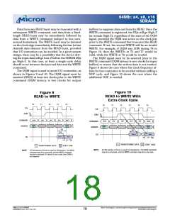
64Mb : x4, x8, x16
SDRAM
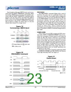
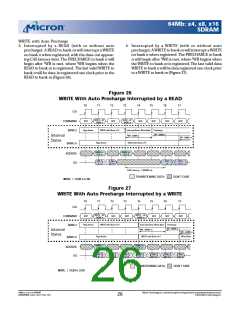
Data for any WRITE burst m ay be truncated with a
subsequent READ com m and, and data for a fixed-
length WRITE burst m ay be im m ediately followed by a
subsequent READ com m and. Once the READ com -
m and is registered, the data inputs will be ignored, and
WRITEs will not be executed. An exam ple is shown in
Figure 17. Data n + 1 is either the last of a burst of two or
the last desired of a longer burst.
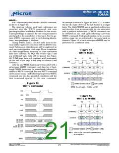
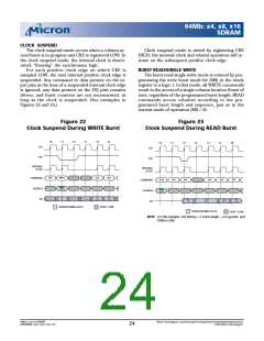
Data for a fixed-length WRITE burst m ay be fol-
lowed by, or truncated with, a PRECHARGE com m and
to the sam e bank (provided that auto precharge was
not activated), and a full-page WRITE burst m ay be
truncated with a PRECHARGE com m and to the sam e
bank. The PRECHARGE com m and should be issued
tWR after the clock edge at which the last desired input
data elem ent is registered. The auto precharge m ode
requires a tWR of at least one clock plus tim e, regardless
of frequency. In addition, when truncating a WRITE
burst, the DQM signal m ust be used to m ask input data
for the clock edge prior to, and the clock edge coinci-
dent with, the PRECHARGE com m and. An exam ple is
shown in Figure 18. Data n + 1 is either the last of a burst
of two or the last desired of a longer burst. Following the
PRECHARGE com m and, a subsequent com m and to
t
the sam e bank cannot be issued until RP is m et.
In the case of a fixed-length burst being executed to
com pletion, a PRECHARGE com m and issued at the
optim um tim e (as described above) provides the sam e
operation that would result from the sam e fixed-length
burst with auto precharge. The disadvantage of the
PRECHARGE com m and is that it requires that the com -
m and and address buses be available at the appropri-
ate tim e to issue the com m and; the advantage of the
PRECHARGE com m and is that it can be used to trun-
cate fixed-length or full-page bursts.
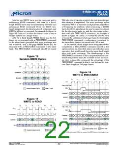
Fig u re 16
Ra n d o m WRITE Cycle s
T0
T1
T2
T3
CLK
WRITE
WRITE
WRITE
WRITE
Fig u re 18
WRITE t o PRECHARGE
COMMAND
ADDRESS
DQ
BANK,
COL n
BANK,
COL a
BANK,
COL x
BANK,
COL m
T0
T1
T2
T3
T4
T5
T6
CLK
D
IN
D
IN
D
IN
DIN
m
n
a
x
t
t
WR @ CLK ≥ 15ns
DQM
DON’T CARE
TRANSITIONING DATA
t
RP
NOP
NOP
NOP
WRITE
NOP
PRECHARGE
ACTIVE
COMMAND
ADDRESS
BANK
(a or all)
BANK a,
COL n
BANK a,
ROW
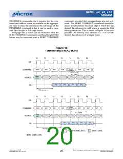
Fig u re 17
WRITE t o READ
t
WR
D
n
IN
DIN
n + 1
DQ
T0
T1
T2
T3
T4
T5
t
t
WR = CLK < 15ns
CLK
DQM
t
RP
WRITE
NOP
READ
NOP
NOP
NOP
COMMAND
ADDRESS
DQ
NOP
NOP
WRITE
NOP
NOP
PRECHARGE
ACTIVE
COMMAND
ADDRESS
BANK
(a or all)
BANK a,
COL n
BANK a,
ROW
BANK,
COL n
BANK,
COL b
t
WR
D
n
IN
DIN
n + 1
DQ
DIN
DIN
DOUT
DOUT
b + 1
n
n + 1
b
DON’T CARE
TRANSITIONING DATA
DON’T CARE
TRANSITIONING DATA
NOTE: DQM could remain LOW in this example if the WRITE burst is a fixed length of two.
64Mb: x4, x8, x16 SDRAM
64MSDRAM_F.p65 – Rev. F; Pub. 1/03
Micron Technology, Inc., reservesthe right to change productsor specificationswithout notice.
©2003, Micron Technology, Inc.
22

 MICRON [ MICRON TECHNOLOGY ]