64Mb : x4, x8, x16
SDRAM
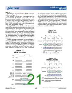
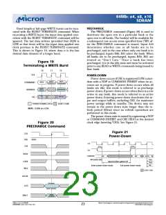
Fixed-length or full-page WRITE bursts can be trun-
cated with the BURST TERMINATE com m and. When
truncating a WRITE burst, the input data applied coin-
cident with the BURST TERMINATE com m and will be
ignored. The last data written (provided that DQM is
LOW at that tim e) will be the input data applied one
clock previous to the BURST TERMINATE com m and.
This is shown in Figure 19, where data n is the last
desired data elem ent of a longer burst.
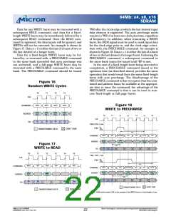
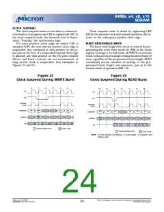
PRECHARGE
The PRECHARGE com m and (Figure 20) is used to
deactivate the open row in a particular bank or the
open row in all banks. The bank(s) will be available for
a subsequent row access som e specified tim e (tRP) af-
ter the PRECHARGE com m and is issued. Input A10
d eterm in es wh eth er on e or all b an ks are to b e
precharged, and in the case where only one bank is to
be precharged, inputs BA0, BA1 select the bank. When
all banks are to be precharged, inputs BA0, BA1 are
treated as “Don ’t Care.” On ce a b an k h as b een
precharged, it is in the idle state and m ust be activated
prior to any READ or WRITE com m ands being issued to
that bank.
Fig u re 19
Te rm in a t in g a WRITE Bu rst
T0
T1
T2
CLK
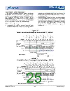
POWER-DOWN
Power-down occurs if CKE is registered LOW coinci-
dent with a NOP or COMMAND INHIBIT when no ac-
cesses are in progress. If power-down occurs when all
banks are idle, this m ode is referred to as precharge
power-down; if power-down occurs when there is a row
active in any bank, this m ode is referred to as active
power-down. Entering power-down deactivates the in-
put and output buffers, excluding CKE, for m axim um
power savings while in standby. The device m ay not
rem ain in the power-down state longer than the re-
fresh period (64m s) since no refresh operations are
perform ed in this m ode.
BURST
TERMINATE
NEXT
COMMAND
WRITE
COMMAND
ADDRESS
DQ
BANK,
COL n
(ADDRESS)
(DATA)
DIN
n
TRANSITIONING DATA
DON’T CARE
NOTE: DQMs are LOW.
The power-down state is exited by registering a NOP
or COMMAND INHIBIT and CKE HIGH at the desired
t
clock edge (m eeting CKS). See Figure 21.
Fig u re 20
PRECHARGE Co m m a n d
Fig u re 21
CLK
Po w e r-Do w n
CKE
CS#
HIGH
( (
) )
CLK
( (
) )
> t
CKS
t
CKS
CKE
( (
) )
RAS#
( (
) )
COMMAND
NOP
NOP
ACTIVE
( (
) )
t
All banks idle
RCD
RAS
RC
CAS#
WE#
Input buffers gated off
t
t
Enter power-down mode.
Exit power-down mode.
DON’T CARE
A0-A9
A10
All Banks
Bank Selected
BANK
ADDRESS
BA0,1
64Mb: x4, x8, x16 SDRAM
64MSDRAM_F.p65 – Rev. F; Pub. 1/03
Micron Technology, Inc., reservesthe right to change productsor specificationswithout notice.
©2003, Micron Technology, Inc.
23

 MICRON [ MICRON TECHNOLOGY ]