64Mb : x4, x8, x16
SDRAM
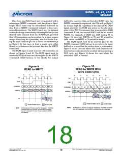
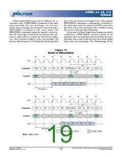
Data from any READ burst m ay be truncated with a
subsequent WRITE com m and, and data from a fixed-
length READ burst m ay be im m ediately followed by
data from a WRITE com m and (subject to bus turn-
around lim itations). The WRITE burst m ay be initiated
on the clock edge im m ediately following the last (or last
desired) data elem ent from the READ burst, provided
that I/ O contention can be avoided. In a given system
design, there m ay be a possibility that the device driv-
ing the input data will go Low-Z before the SDRAM DQs
go High-Z. In this case, at least a single-cycle delay
should occur between the last read data and the WRITE
com m an d.
buffers) to suppress data-out from the READ. Once the
WRITE com m and is registered, the DQs will go High-Z
(or rem ain High-Z), regardless of the state of the DQM
signal, provided the DQM was active on the clock just
prior to the WRITE com m and that truncated the READ
com m and. If not, the second WRITE will be an invalid
WRITE. For exam ple, if DQM was LOW during T4 in
Figure 10, then the WRITEs at T5 and T7 would be
valid, while the WRITE at T6 would be invalid.
The DQM signal m ust be de-asserted prior to the
WRITE com m and (DQM latency is zero clocks for input
buffers) to ensure that the written data is not m asked.
Figure 9 shows the case where the clock frequency al-
lows for bus contention to be avoided without adding a
NOP cycle, and Figure 10 shows the case where the
additional NOP is needed.
The DQM input is used to avoid I/ O contention, as
shown in Figures 9 and 10. The DQM signal m ust be
asserted (HIGH) at least two clocks prior to the WRITE
com m an d (DQM laten cy is two clocks for ou tp u t
Fig u re 10
Fig u re 9
READ t o WRITE Wit h
Ext ra Clo ck Cycle
READ t o WRITE
T0
T1
T2
T3
T4
T0
T1
T2
T3
T4
T5
CLK
CLK
DQM
DQM
READ
NOP
NOP
NOP
WRITE
COMMAND
ADDRESS
READ
NOP
NOP
NOP
NOP
WRITE
COMMAND
ADDRESS
BANK,
COL n
BANK,
COL b
BANK,
COL b
BANK,
COL n
t
CK
t
HZ
t
HZ
D
OUT
n
DIN
b
DQ
DOUT
n
DIN b
DQ
t
DS
t
DS
TRANSITIONING DATA
DON’T CARE
TRANSITIONING DATA
DON’T CARE
NOTE:
A CAS latency of three is used for illustration. The READ command
may be to any bank, and the WRITE command may be to any bank.
NOTE:
A CAS latency of three is used for illustration. The READ
command may be to any bank, and the WRITE command
may be to any bank. If a burst of one is used, then DQM is
not required.
64Mb: x4, x8, x16 SDRAM
64MSDRAM_F.p65 – Rev. F; Pub. 1/03
Micron Technology, Inc., reservesthe right to change productsor specificationswithout notice.
©2003, Micron Technology, Inc.
18

 MICRON [ MICRON TECHNOLOGY ]