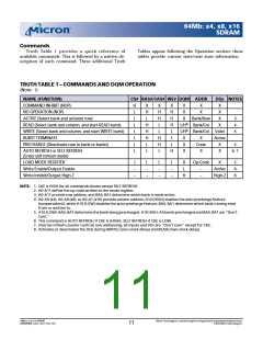
64Mb : x4, x8, x16
SDRAM
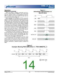
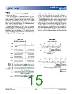
READs
READ bursts are initiated with a READ com m and,
as shown in Figure 5.
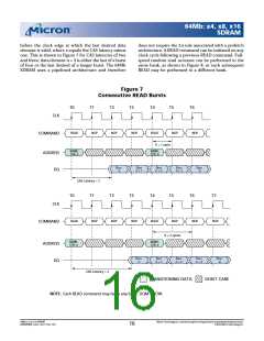
Upon com pletion of a burst, assum ing no other com -
m ands have been initiated, the DQs will go High-Z. A
full-page burst will continue until term inated. (At the
end of the page, it will wrap to colum n 0 and continue.)
Data from any READ burst m ay be truncated with a
subsequent READ com m and, and data from a fixed-
length READ burst m ay be im m ediately followed by
data from a READ com m and. In either case, a continu-
ous flow of data can be m aintained. The first data ele-
m ent from the new burst follows either the last ele-
m ent of a com pleted burst or the last desired data ele-
m en t of a lon ger bu rst wh ich is bein g tru n cated.
The new READ com m and should be issued x cycles
The starting colum n and bank addresses are pro-
vided with the READ com m and, and auto precharge is
either enabled or disabled for that burst access. If auto
p rech arge is en ab led , th e row b ein g accessed is
precharged at the com pletion of the burst. For the ge-
neric READ com m ands used in the following illustra-
tions, auto precharge is disabled.
During READ bursts, the valid data-out elem ent
from the starting colum n address will be available fol-
lowing the CAS latency after the READ com m and. Each
subsequent data-out elem ent will be valid by the next
positive clock edge. Figure 6 shows general tim ing for
each possible CAS latency setting.
Fig u re 5
Fig u re 6
READ Co m m a n d
CAS La t e n cy
T0
T1
T2
T3
CLK
CLK
CKE
CS#
HIGH
COMMAND
READ
NOP
t
NOP
t
LZ
OH
DOUT
DQ
t
AC
CAS Latency = 2
RAS#
CAS#
WE#
T0
T1
T2
T3
T4
CLK
COMMAND
READ
NOP
NOP
NOP
t
t
LZ
OH
A0-A9: x4
A0-A8: x8
A0-A7: x16
COLUMN
ADDRESS
DOUT
DQ
t
AC
A11: x4
A9, A11: x8
A8, A9, A11: x16
CAS Latency = 3
DON’T CARE
UNDEFINED
ENABLE AUTO PRECHARGE
DISABLE AUTO PRECHARGE
A10
BANK
ADDRESS
BA0,1
64Mb: x4, x8, x16 SDRAM
64MSDRAM_F.p65 – Rev. F; Pub. 1/03
Micron Technology, Inc., reservesthe right to change productsor specificationswithout notice.
©2003, Micron Technology, Inc.
15

 MICRON [ MICRON TECHNOLOGY ]