64Mb : x4, x8, x16
SDRAM
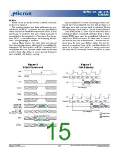
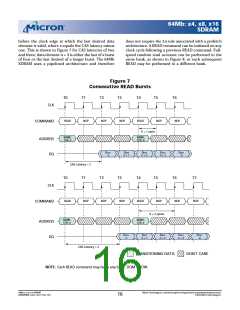
before the clock edge at which the last desired data
elem ent is valid, where x equals the CAS latency m inus
one. This is shown in Figure 7 for CAS latencies of two
and three; data elem ent n + 3 is either the last of a burst
of four or the last desired of a longer burst. The 64Mb
SDRAM uses a pipelined architecture and therefore
does not require the 2n rule associated with a prefetch
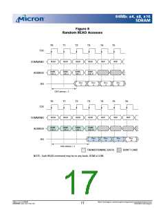
architecture. A READ com m and can be initiated on any
clock cycle following a previous READ com m and. Full-
speed random read accesses can be perform ed to the
sam e bank, as shown in Figure 8, or each subsequent
READ m ay be perform ed to a different bank.
Fig u re 7
Co n se cu t ive READ Bu rst s
T0
T1
T2
T3
T4
T5
T6
CLK
READ
NOP
NOP
NOP
READ
NOP
NOP
COMMAND
X = 1 cycle
BANK,
COL n
BANK,
COL b
ADDRESS
DQ
D
OUT
D
n + 1
OUT
DOUT
DOUT
DOUT
n
n + 2
n + 3
b
CAS Latency = 2
T0
T1
T2
T3
T4
T5
T6
T7
CLK
READ
NOP
NOP
NOP
READ
NOP
NOP
NOP
COMMAND
X = 2 cycles
BANK,
COL n
BANK,
COL b
ADDRESS
DQ
D
OUT
DOUT
DOUT
DOUT
DOUT
n
n + 1
n + 2
n + 3
b
CAS Latency = 3
TRANSITIONING DATA
DON’T CARE
NOTE: Each READ command may be to any bank. DQM is LOW.
64Mb: x4, x8, x16 SDRAM
64MSDRAM_F.p65 – Rev. F; Pub. 1/03
Micron Technology, Inc., reservesthe right to change productsor specificationswithout notice.
©2003, Micron Technology, Inc.
16

 MICRON [ MICRON TECHNOLOGY ]