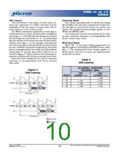
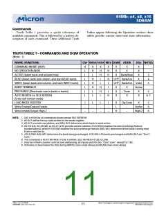
64Mb : x4, x8, x16
SDRAM
Op e ra t io n
Fig u re 3
Act iva t in g a Sp e cific Ro w in a
Sp e cific Ba n k
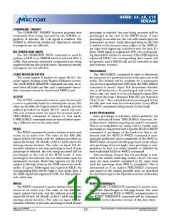
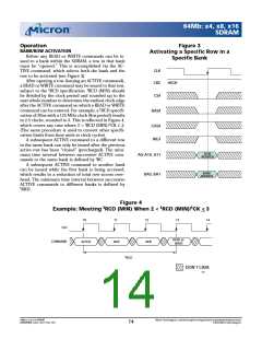
BANK/ROW ACTIVATION
Before any READ or WRITE com m ands can be is-
sued to a bank within the SDRAM, a row in that bank
m ust be “opened.” This is accom plished via the AC-
TIVE com m and, which selects both the bank and the
row to be activated (see Figure 3).
CLK
After opening a row (issuing an ACTIVE com m and),
a READ or WRITE com m and m ay be issued to that row,
CKE
CS#
HIGH
t
t
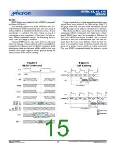
subject to the RCD specification. RCD (MIN) should
be divided by the clock period and rounded up to the
next whole num ber to determ ine the earliest clock edge
after the ACTIVE com m and on which a READ or WRITE
t
com m and can be entered. For exam ple, a RCD specifi-
RAS#
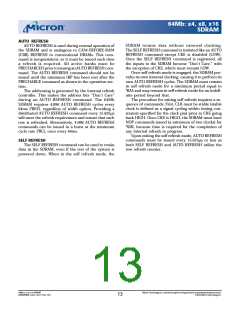
cation of 20ns with a 125 MHz clock (8ns period) results
in 2.5 clocks, rounded to 3. This is reflected in Figure 4,
t
which covers any case where 2 < RCD (MIN)/ tCK £ 3.
CAS#
WE#
(The sam e procedure is used to convert other specifi-
cation lim its from tim e units to clock cycles).
A subsequent ACTIVE com m and to a different row
in the sam e bank can only be issued after the previous
active row has been “closed” (precharged). The m ini-
m um tim e interval between successive ACTIVE com -
ROW
ADDRESS
A0–A10, A11
BA0, BA1
t
m ands to the sam e bank is defined by RC.
A subsequent ACTIVE com m and to another bank
can be issued while the first bank is being accessed,
which results in a reduction of total row-access over-
head. The m inim um tim e interval between successive
ACTIVE com m ands to different banks is defined by
tRRD.
BANK
ADDRESS
Fig u re 4
Exa m p le : Me e t in g RCD (MIN) Wh e n 2 < RCD (MIN)/ CK < 3
t
t
t
T0
T1
T2
T3
T4
CLK
READ or
WRITE
COMMAND
ACTIVE
NOP
NOP
t
RCD
DON’T CARE
64Mb: x4, x8, x16 SDRAM
64MSDRAM_F.p65 – Rev. F; Pub. 1/03
Micron Technology, Inc., reservesthe right to change productsor specificationswithout notice.
©2003, Micron Technology, Inc.
14

 MICRON [ MICRON TECHNOLOGY ]