1Gb: x4, x8, x16 DDR2 SDRAM
Functional Description
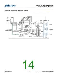
Functional Description
The DDR2 SDRAM uses a double data rate architecture to achieve high-speed opera-
tion. The double data rate architecture is essentially a 4n-prefetch architecture, with an
interface designed to transfer two data words per clock cycle at the I/O balls. A single
read or write access for the DDR2 SDRAM effectively consists of a single 4n-bit-wide, one-
clock-cycle data transfer at the internal DRAM core and four corresponding n-bit-wide,
one-half-clock-cycle data transfers at the I/O balls.
A bidirectional data strobe (DQS, DQS#) is transmitted externally, along with data, for
use in data capture at the receiver. DQS is a strobe transmitted by the DDR2 SDRAM
during READs and by the memory controller during WRITEs. DQS is edge-aligned with
data for READs and center-aligned with data for WRITEs. The x16 offering has two data
strobes, oneforthelowerbyte(LDQS, LDQS#)andonefortheupperbyte(UDQS, UDQS#).
The DDR2 SDRAM operates from a differential clock (CK and CK#); the crossing of CK
going HIGH and CK# going LOW will be referred to as the positive edge of CK. Com-
mands (address and control signals) are registered at every positive edge of CK. Input
data is registered on both edges of DQS, and output data is referenced to both edges of
DQS as well as to both edges of CK.
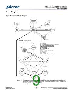
Read and write accesses to the DDR2 SDRAM are burst-oriented; accesses start at a se-
lected location and continue for a programmed number of locations in a programmed
sequence. Accesses begin with the registration of an ACTIVATE command, which is
then followed by a READ or WRITE command. The address bits registered coincident
with the ACTIVATE command are used to select the bank and row to be accessed. The
address bits registered coincident with the READ or WRITE command are used to select
the bank and the starting column location for the burst access.
The DDR2 SDRAM provides for programmable read or write burst lengths of four or
eight locations. DDR2 SDRAM supports interrupting a burst read of eight with another
read or a burst write of eight with another write. An auto precharge function may be
enabled to provide a self-timed row precharge that is initiated at the end of the burst
access.
As with standard DDR SDRAM, the pipelined, multibank architecture of DDR2 SDRAM
enables concurrent operation, thereby providing high, effective bandwidth by hiding
row precharge and activation time.
A self refresh mode is provided, along with a power-saving, power-down mode.
All inputs are compatible with the JEDEC standard for SSTL_18. All full drive-strength
outputs are SSTL_18-compatible.
Industrial Temperature
The industrial temperature (IT) option, if offered, has two simultaneous requirements:
ambient temperature surrounding the device cannot be less than –40°C or greater than
+85°C, and the case temperature cannot be less than –40°C or greater than +95°C. JE-
DEC specifications require the refresh rate to double when TC exceeds +85°C; this also
requires use of the high-temperature self refresh option. Additionally, ODT resistance
and the input/output impedance must be derated when TC is < 0°C or > +85°C.
PDF: 09005aef821ae8bf
1GbDDR2.pdf – Rev. T 02/10 EN
Micron Technology, Inc. reserves the right to change products or specifications without notice.
10
© 2004 Micron Technology, Inc. All rights reserved.

 MICRON [ MICRON TECHNOLOGY ]