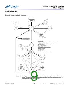
1Gb: x4, x8, x16 DDR2 SDRAM
Functional Block Diagrams
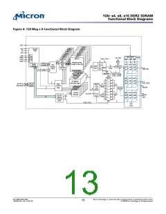
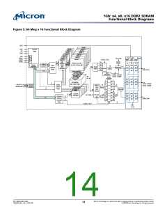
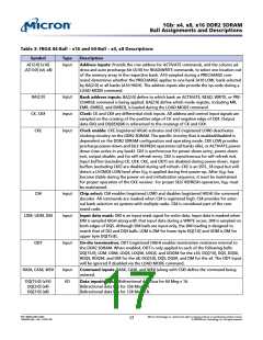
Figure 4: 128 Meg x 8 Functional Block Diagram
ODT
Bank 7
Bank 6
CKE
CK
CK#
Bank 7
Bank 6
Control
logic
Bank 5
Bank 5
Bank 4
Bank 4
Bank 3
Bank 3
Bank 2
Bank 1
CS#
RAS#
CAS#
WE#
Bank 2
ODT control
Vdd Q
CK, CK#
DLL
Bank 1
Bank 0
COL0, COL1
MUX
sw1 sw2 sw3
Bank 0
14
row-
address
latch
8
8
8
8
Memory array
(16,384 x 256 x 32)
Refresh
counter
16,384
14
Mode
registers
sw1 sw2 sw3
Row-
address
MUX
8
32
and
decoder
Read
latch
DRVRS
R1
R1
R2
R2
R3
R3
Data
17
DQ0–DQ7
14
Sense amplifers
8,192
2
DQS
generator
UDQS, UDQS#
LDQS, LDQS#
32
Input
registers
2
sw1 sw2 sw3
2
2
R1
R1
R2
R2
R3
R3
I/O gating
DM mask logic
2
2
2
8
8
8
8
2
DQS, DQS#
RDQS#
A0–A13,
BA0–BA2
2
4
Address
register
Bank
control
logic
WRITE
FIFO
and
17
2
Mask
3
256
(x32)
2
RCVRS
32
drivers
8
sw1 sw2 sw3
Column
decoder
8
8
CK out
CK in
32
CK,CK#
RDQS
DM
R1
R1
R2
R2
R3
R3
Column-
address
counter/
latch
8
8
Data
10
2
8
2
COL0, COL1
Vss Q
PDF: 09005aef821ae8bf
1GbDDR2.pdf – Rev. T 02/10 EN
Micron Technology, Inc. reserves the right to change products or specifications without notice.
13
© 2004 Micron Technology, Inc. All rights reserved.

 MICRON [ MICRON TECHNOLOGY ]